There are several procedures for measurement of the basic parameters of an operational amplifier. Here, we will describe few of them using simulation and theory approach, but these procedures can be also executed with real components, too. So, let's start with measurement of the parameter Avo - the open loop voltage amplification. The circuit configuration used for this measurement procedure is shown on the Picture 1.
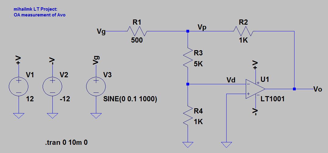
Picture 1: Measurement of the parameter Avo
In order to escape the direct determination of the Avo amplification, we can use the circuit from Picture 1. Here, we assume that the voltage offset compensation is previously done. Namely, the voltage offset is defined as a small differential voltage applied to the inputs to force the output to zero, and also, the voltage offset compensation means providing zero output voltage when there is no input voltage. One simple procedure for voltage offset compensation is as follows: we provide power supply to the OA - usually it's bi-pole supply +/- V; then we connect both inputs of the OA to each other which results in one single input; under these conditions, we measure the output voltage of the OA and if it's not equal to zero volts that means that we have a voltage offset which need to be compensate; depending of the components type that we use (some OA has dedicated pinouts for connecting external trimmer resistor for adjusting the offset), we should start changing the potential of one of the power supply voltages +/- V, or of both, and keep changing them until output voltage is equal to zero (Vo = 0). Now, back to the measurement procedure for Avo, we also assume that the generator signal Vg is selected with lower frequency than the frequency of the predominant pole of the OA and with amplitude which will not bring the OA into non-linear working mode. Finally, the voltage amplification can be found according to this relation:
Avo = Vo/Vp(1 + R3/R4)
Transient Analysis
Using transient (time domain) analysis in DC sweep mode in LT Spice we measure the transient characteristic of the circuit configuration. The result is shown on Picture 2. On x-axis we have the input DC voltage and on y-axis we have the output voltage Vo. The input voltage is changing in the range from -100 mV to 100 mV with step of 10 mV. For this purpose we run DC sweep simulation in LT Spice which computes the DC operating point of a circuit while stepping independent source and treating capacitances as open circuits and inductances as short circuits. The parameters settings of our DC sweep simulation are:
Source to sweep: Vi (it's attached to the inverting input of the OA);
Type of sweep: Linear;
Start Value: -100 mV;
Stop Value: +100 mV;
Increment: 10 mV;
The syntax of the simulation command used for this transient analysis is: .dc Vi -0.1 0.1 0.01
Picture 2: Transient characteristic of the OA circuit
As we can see from the plot shown on Picture 2, we have a zero volts on the output Vo = 0 V, when the input is +5 mV. When the input is +10 mV we have about -11 V on the output, and when the input is 0 V we have about +11 V on the output. For the input voltages less than 0 V the output remains constant at value of 11 V, and for input voltages greater than 10 mV the output voltage remains constant at value of -11 V. So, according to the simulation results, we can resume that the voltage offset for this circuit configuration is +5 mV. In other words, we need to bring +5 mV on the input of the operational amplifier in order to have zero volts on its output.
AC Analysis
The phase-frequency characteristics of this circuit were measured with AC analysis in LT spice. LT Spice computes the small signal AC behavior of the circuit linearized about its DC operating point. In this AC simulation were used these parameters:
Type of Sweep: Octave;
Number of points per octave: 1;
Start Frequency: 20 Hz;
Stop Frequency: 10 MHz;

Picture 3: AC Analysis - output voltage [dB] and its phase [degrees] (frequency-domain)
The frequency-domain characteristic of our circuit configuration is shown on the Picture 3. The magnitude of the output voltage is 6 dB for frequencies of the input signal up to 10 kHz. The amplification decreases for 3 dB from its maximum value at frequency of about 46 kHz, which is actually the dominant frequency pole for this circuit configuration.
The common mode rejection ratio - CMRR
The common mode rejection ratio - CMRR is defined same way as it was defined for the differential amplifier, with the ratio between the differential and the synphase amplification:
CMRR = Avo/Avcm

Picture 4: Measurement of the parameter CMRR factor
The CMRR parameter can be determined directly from the circuit shown on Picture 4, using the following relation:
CMRR = Vicm/Vid = Vg/Vo(1 + R2/R1)
There are also procedures for measurement of the input and output resistance/impedance of the circuit, but here we will not consider them. The above explained measurement procedures are only simple theory approach, but the same concepts can be applied for every circuit configuration depending on its design and purpose.
No comments:
Post a Comment