Blocking oscillator is a one-step relaxation generator with strong positive feedback, which is inductive and implemented with pulse transformer. The pulse transformer is the basic accumulation element of the assembly, and it has high inductance of magnetization of the primary coil, low leakage inductance, or low capacitance of the coils.
Since the pulse transformer is constructed with coefficient of coupling:
K = M/sqrt(Lp*Ls)
with value near to 1, where M is inter-inductance or mutual inductunce, Lp is primary inductance and Ls is secondary inductance. The transfer ratio of the transformer is defined as:
n = Vs/Vp = Ip/Is = Ns/Np = sqrt(Ls)/sqrt(Lp)
Here, the Ns and Np are the numbers of turns in secondary and primary coils, respectively. Vs, Vp and Is, Ip are the voltages and currents in the secondary and primary coils.
The blocking oscillator may generate short-time pulses with high frequency and high available power. Because of the strong positive feedback, the slope edge of the pulses is exceptionally high, while with application of third coil in the transformer it can be provided a generating of pulses with different amplitude and polarity. Depending on the set point for the DC mode of the active element, the blocking oscillator can work as monostable or astable assembly.

Picture 1: Monostable Blocking Oscillator circuit
On Picture 1 is shown an blocking oscillator in monostable mode provided with the negative voltage source applied to the base of the transistor and which the transistor in the blocking region, but because of the non-zero conduction threshold of the transistor, it takes that Vbb = 0, i.e. the base resistor can be connected to the ground. The activating of the transistor can be done if positive rise of its base voltage is provided. In our circuit, that's done with additional triggering transistor Q2, when it is lead to saturation which generates positive rise of the voltage in the base coil of the pulse transformer, L1.
We have to mention here, that the transformer element in LT spice can be configured as two, or more inductors depending of the number of coils of the transformer, and in order to specify the mutual inductunce by which actually we couple the inductors to act as a transformer, we need to insert a spice directive into our circuit in LT Spice with letter "K". After the letter K, we specify the coils that form the transformer and at the end we specify the mutual coupling coefficient, which value can goes from 0 to 1, where 1 means perfect coupling or in other words, no leakage inductance. Since we are simulating the circuit, the perfect coupling for the transformer we use would be just fine, so the spice directive for the model of the pulse transformer that we need to simulate in our circuit, as is shown on Picture 1, would be: "K L1 L2 1".
When the transistor Q1 exits the saturation mode, the accumulated charge in its base results in negative rise of the base current, while the accumulated energy of magnetization of the transformer coil L2 leads to positive rise of the collector voltage. In order to decrease these effects, the diode D is connected on the transformer coil L2.
Time-domain analysis
The results of the transient analysis for this circuit in time domain are shown on Picture 2 and Picture 3. The triggering signal applied to this circuit, VT is configured as sinusoidal signal with amplitude of 10 V at frequency of 500 Hz.
A. Transient analysis I
For this analysis, we use the negative or zero voltage for the voltage source Vbb. In our case, we set the Vbb = -5 V, but the same result can be achieved in case when Vbb = 0 V. So, with negative Vbb voltage, the output voltage of the circuit has slow and small oscillations, as shown on Picture 2. The output voltage varies around the 12 V with relative peaks of about +/- 60 mV. The time duration between two positive peaks is about 2 ms, which is corresponding to the frequency of 500 Hz, and that's exactly the frequency of the triggering signal.
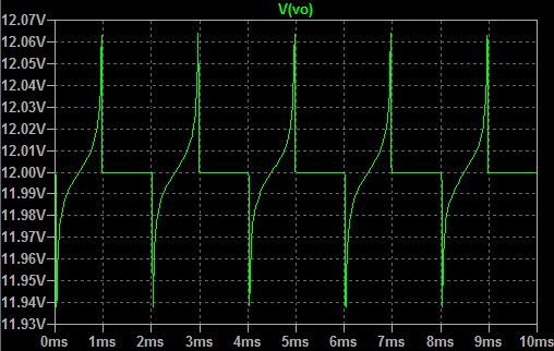
Picture 2: Transient analysis I - output voltage Vo wave form (time-domain)
B. Transient analysis II
In this second analysis, we use the positive voltage for the voltage source Vbb, and in this case we set it to Vbb = +10 V. As it can be seen from Picture 3, the output voltage has periods of non-oscillating and oscillating states. Starting with non-oscillating state it changes between these states each milisecond, so it has stable value around 12 V for 1 ms, then starts oscillating between 14 and 1 V values for the next 1 ms, and so on. The zoom in of the wave form of Vo, is shown on Picture 4, where the oscillations of the voltage are noticeable.

Picture 3: Transient analysis II - output voltage Vo wave form (time-domain)
The high level of the output voltage starts with peak of about 14 V, then falls to about 12.75 V just before it enters the short negative peak of its low level, which is at around 1 V. The time duration between two peaks of the output voltage is about 1.3 us which corresponds to the frequency of about 769 kHz, and that's 1538 times greater frequency than the initial frequency of 500 Hz of the triggering pulse VT. This way, the monostable blocking oscillator circuit can be used to produce pulses with different frequency, in our case much higher than the frequency of the triggering voltage.

Picture 4: Transient analysis II - Zoom In of output voltage Vo wave form (time-domain)
No comments:
Post a Comment