The method of utilization of the radio waves energy is kind of a derived idea from the
Tesla's Method Of Utilizing Radiant Energy, as general concept. In this article, we analyze one simple electronic circuit which can be used as simple prototype for proving the concept of utilization of the energy of radio waves which propagates in the Earth's atmosphere all the time. These radio waves does not have a mysterious origin at all, as it can be found in many places on the internet sites which treats the so called "free energy" phenomenon. On the contrary, these radio waves are just real and known, human made signals. They origin from the base and repeater stations of the broadcasting network, comprising emitters of all local and national radio stations. The signal emitted from your favorite radio station which broadcasts program with music and news of your interest, is always present in the air around you, no matter if you catch that signal on your radio and listen its live program, or your radio is turned off. That signal is always there. And not just the signal from that particular radio station, which is your favorite, but also and all the other stations that emit their signals in your near or far environment.
So, if you chose not to listen the radio, that doesn't mean that you can not catch the radio signals around you, and try to utilize or store the energy that they carry out with them. Although this energy is relatively small, it can still be detected and accumulated on proper way, just as a proving fact that it exists in the air. Furthermore, since we know the origin of these radio waves, we can't say that the energy they carry around is "free", because we know that this energy is generated in the transmitter stations of the radio service which generated it. These radio transmitters doesn't work from nothing, they use electric power to generate the needed EM energy of the radio waves which they broadcast via the antennas, in their well known and pre-calculated range. Of course, the radio station is paying for the electric energy that it consumes, but the very small portion of the emitted EM energy that comes to your radio receiver via its receiver antenna at your home, you get it for free. However, this received energy is far different from the term "free energy" and its actual meaning.
The receiving circuit for utilizing radio waves energy
Let's now take a look at one real and simple circuit, which can accumulate the EM energy of radio waves via the receiving antenna. The utilization circuit is shown on
Picture 1. The electrolytic capacitors C3 and C4 are used as elements for storing the energy, as they accumulate the charge from the incoming small-amplitude radio signals via the diode network which is constructed with 4 diodes D1, D2, D3 and D4, connected as shown in circuit (
Picture 1). The capacity of the energy storing capacitors are set to relatively huge value of 1000 μF. The radio signals received from the antenna, are passed to the diode network via the signal block capacitors C1 and C2. Their value is set to 22 nF. Since we are simulating this circuit, we also need to simulate and the antenna as the most important circuit element here.
An antenna is best modeled as a voltage source with a fixed value of internal resistance. Generally, that is the radiation resistance of the antenna. So, in our circuit, we modeled the receiving antenna as a simple voltage source, with the series resistance value of 50 ohms. Although the voltage level of real radio waves is very small, we chose the value of magnitudes in this simulation which is far more higher, just for analyzing purposes. However, the concept of functioning of this circuit and its effect, will remain the same and for smaller and real values for the magnitudes of the incoming radio waves, except that the resulting values of the output voltage V+, will be much smaller, accordingly to the input signal values. But the important thing here, is to see that this idea as concept for utilization of the energy, really works. Therefore, for the antenna model used in our simulation, we use simple sinusoidal wave form, with magnitude of 200 mV at frequency of 500 kHz.
Picture 1: Utilization of Radio Waves Energy (simple circuit)
Time-domain analysis
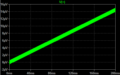
The results of the transient analysis for this circuit in time domain are shown on
Picture 2. For this analysis, the same simple sinusoidal wave form, with magnitude of 200 mV at frequency of 500 kHz, is used for antenna signal. As it can be seen from the plot, the output voltage level starts increasing with oscillating wave form, according to the input signal frequency. Starting from zero, the output level reaches value of about 14 μV after time period of 200 ms. The increasing rate is almost linear, so, after time period of 1 second, output will increase to value around 70 μV. This value is about 0.00035% of the input signal magnitude value. In other words, it's far more less than the input. So, in order to achieve really measurable voltage on the output of this circuit, the circuit should work for a long time, thus accumulating energy constantly. We have implemented one real prototype of this circuit, and the real results from practice showed us that the circuit should be left in accumulating mode for, let's say a period of one whole day, in order to achieve a value of several up to hundreds of mV on its output.
The above results are in case of single-frequency input signal. As we now, in practice, the antenna will receive more than one signal, and all signals will have different frequencies. Furthermore, these signals are not simple and with pure sinusoidal form, since they are modulated in the proper modulation technique for radio transmission. So, the actual input signal received from the real antenna, would be a superposition of all radio signals that the antenna can receive in the environment where it is installed. However, for analysis purposes, we modeled another type of input antenna, which consists three different voltage sources connected in parallel, just to see the effect of the superposition of several signals at different frequencies. In our case, we set these three voltage sources with the following properties:
>>
V1 voltage source: Frequency:
500 kHz; Amplitude: 200 mV; Wave form: sinusoidal;
>>
V2 voltage source: Frequency:
100 kHz; Amplitude: 200 mV; Wave form: sinusoidal;
>>
V3 voltage source: Frequency:
1 MHz; Amplitude: 200 mV; Wave form: sinusoidal;
Picture 3: Transient analysis - output voltage V+ wave form and input signal from Antenna (time-domain) - for 3 inputs at different frequencies
The resulting input signal wave form of the antenna is shown on
Picture 3. On same plot is shown and the output voltage V+. As it can be seen, although all three input signals have same magnitude of 200 mV, because of their different frequencies, the resulting signal has amplitudes less then 200 mV. The final effect of this superposition is that the output voltage is increasing with slower rate, comparing with the previous case of one single-frequency input signal. So, after the time period of 200 ms, the output level will reach value smaller than 14 μV, as it reached in the previous case (
Picture 2).
AC Analysis
The output voltage AC analysis of this circuit shows that it has higher output level as the frequency of the signal increase. For this AC analysis we set the frequency range of the input signal from 10 KHz to 10 GHz. Taking into account the whole
Radio Spectrum which covers frequencies from 3 Hz up to 3000 GHz, this range that we analyze here is pretty much wide. The output voltage level at frequency of 10 KHz is -144 dB and it increases in linear mode up to frequencies of 100 MHz, where it reaches the level of -66 dB. After these frequencies, the output voltage is still increasing, but with slower rate. Finally, for frequencies above 1 GHz it stops to increase and its level remains at about -59 dB. The output level plot in frequency domain is shown on
Picture 4.
Picture 4: AC analysis - output voltage V+ level (frequency-domain) - for single frequency input
Also, it's good to mention here, that in the lower frequency range of the radio spectrum, starting from 3 Hz to 10 KHz the output level is decreasing. Namely, at 3 Hz input signal, the output level is around - 100 dB, then it decreases with different speeds as frequency increases, so at frequency of around 3 kHz, it reaches the minimum level of around - 150 dB. For the frequencies above 3 kHz it starts to increase.
From the above analysis, we can conclude that this concept really works, but the amount of accumulated energy is not what we really expect and need in real applications. Since we talk about energy storing, we actually need amount of stored energy enough to power some small consumer, let's say LED diode light, or something else. In any case, this is just a simple approach of this concept. The circuit for utilization can be upgraded and optimized in many ways, in order to achieve better and usable effect in practice. The circuit can be split in several banks which will store energy from single-frequency signals, which should be previously demodulated and parsed by frequency, of course. Also, the receiving module can be implemented as antenna field, or system with more antennas, placed in some pre-calculated and optimized space constellation in that way that the received energy would be the maximum possible for the current system.
The real prototype of the circuit
Picture 5: The real prototype of the circuit for utilization of the radio waves energy
As we mention above, we have implemented one real prototype of this circuit, for testing and experiment purposes. The real prototype is shown on
Picture 5. On this prototype circuit we have connected two antennas, removed from an old wi-fi repeater. The rest of the circuit elements are same as the circuit we simulated (
Picture 1). Before connecting the antennas on the circuit, which is actually how this circuit is put in operation, we made sure that the energy storing electrolytic capacitors C3 and C4 are totally discharged. After putting the circuit in operation, next day the measured voltage of its output was 273 mV, as shown on
Picture 6.
Picture 6: Measuring the output voltage of the real prototype (after 1 day of accumulation)