With small variations of the Monostable Blocking Oscillator circuit, it can be provided to work into astable mode. The astable blocking oscillator circuit is shown on Picture 1. Its circuit is very simple and it consists of pulse transformer, diode, transistor and emitter resistor. The base of the transistor is positively polarized with the source Vbb, via the transformer coil L1. The source Vbb provides entry for the transistor into its saturation without external triggering pulse, thus in some period of time it generates similar wave form of the collector voltage as the monostable blocking oscillator.

Picture 1: Astable Blocking Oscillator circuit
After the period of saturation, when the transistor enters into active mode of operation with tendency of blocking, the voltage of the collector becomes Vc = Vcc + Vd, where Vd is the voltage threshold conduction of the diode D. Because the diode is conducting, it decreases the accumulated energy in the transformer coil L2, until the moment when the current of magnetization that flows through the L2 passes through zero changing its direction or polarization. At that moment, the diode becomes blocked, but the transistor is conducting starting with the new cycle of working mode.
Time-domain analysis
The results of the transient analysis for this circuit in time domain is shown on Picture 2. The output voltage Vo starts oscillating at about 383 us. The maximal peaks of the voltage are 12.53 V and the minimal peaks are 11.47 V, so the amplitude of oscillating voltage component is 53 mV. The period of oscillation or the time between two positive peaks is around 0.3 us, which corresponds to frequency of 3.33 MHz.
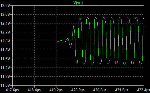
Picture 2: Transient analysis - output voltage Vo wave form (time-domain)
No comments:
Post a Comment