In the common collector amplifier circuit, the common electrode is the collector of the transistor, the input signal leads on the base and the output signal is taken from the emitter. The common collector circuit is shown on Picture 1. This is almost the same circuit configuration as the common emitter circuit that we already analyzed. The only difference here is the connection point of the load (with the output coupling capacitor C2) which is moved (reconnected) from the collector to the emitter of the transistor Q1. Here, again we will use the simplest circuit configuration.
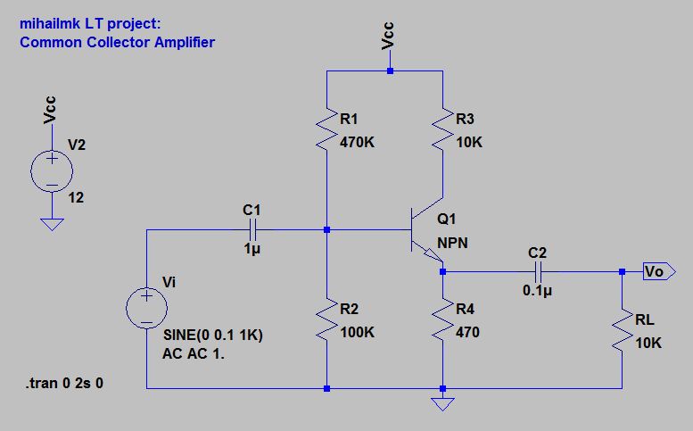
Picture 1: Common Collector Amplifier Circuit
In general, the common collector amplifier circuit has relatively big input impedance and relatively small output impedance. The current amplification is usually big while the voltage amplification is close up to 1, but it's always less than 1. Because the output signal, which is taken from the emitter, is in phase with the input signal in the base of the transistor and it's close to it (since the voltage amplification is near to 1) we can say that the output follows the input. That's the reason why the common collector amplifier circuit is called "emitter follower". Using the simplified hybrid model for the transistor for common emitter circuit (He), the following simplified expressions for voltage and circuit amplification can be found:
Av = Vo/Vi = ( (1 + hfe)*(Re||Rl) ) / ( hie + (1 + hfe)*(Re||Rl) ) , --> for hfe >> 1 => Av ~ 1
Ai = Io/Ii = ( (1 + hfe) / ( 1 + (hie + (1 + hfe)*(Re||Rl))/Rth ) ) * ( Re/(Re + Rl) ) ,
where:
Re||Rl = (Re*Rl)/(Re+Rl) - parallel resistance of the emitter's resistance (Re, in our case R4) and load resistance (Rl);
Rth - is the equivalent Thévenin's resistance of the circuit, looking from its input - this equivalent resistance Rth is the resistance obtained at terminals A-B of the network with all its independent current sources open circuited and all its independent voltage sources short circuited - in our case terminal A is the input point of the circuit - electrode of the C1 and terminal B is the ground;
Time-domain analysis
The transient analysis of the circuit was performed as non-linear time-domain simulation for the first 2 seconds from applying the power supply and input signal. The time domain wave forms of the voltage signals of input and output are shown on the Picture 2. The blue color trace is the input voltage measured right before C1 (actually, that's the Vi waveform) and the green color trace is the output voltage measured right after the C2 (actually, that's the Vo waveform - the voltage of the load Rl). These wave forms are at time moment about 620 ms after the start of the simulation. As we can see from the Picture 2, the output signal is relatively ok, there are not any visible distortions of its wave form. Also, we can see that there is a little phase shift between input and output signals. Now, we can see more precise results from the simulation through the numbers measured in LT Spice (approximate values):
For Vi max = + 100 mV => Vo max = + 92,4 mV;
For Vi min = - 100 mV => Vo min = - 92,9 mV;
--> Av = 0.92 (approximate voltage amplification Av = Vo/Vi)
For Ic1 min = - 4.5 uA => IRl min = - 9.2 uA;
For IC1 max = + 15.7 uA => IRl max = + 9.2 uA;
--> Ai = 2 (approximate current amplification Ai = Io/Ii)
(*Ic1 is the current that flows through capacitor C1, and Irl is the current that flows through the load Rl)

Picture 2: Transient analysis - input and output voltage wave forms (time-domain)
So, according to numbers, min and max values of the output voltage signal vary for about 0.5 mV, which is not big value for the Vo amplitude of about 93 mV (about 0.5 % distortion). The approximate voltage amplification for this circuit configuration is about Av = 0.92, while the approximate current amplification is Ai = 2. Here, we have a big distortion of the input current signal, namely, for the negative half-period of the input signal the input current reaches minimum value of - 4.5 uA, and for the positive half-period it reaches maximum value of + 15.7 uA, which results in sharp positive peaks in the waveform. This is caused by the relatively high voltage level of the input signal for this circuit configuration. The high input voltage level, allows the transistor to enter into the non-linear region for the positive half-period of the signal and that results in the distorted current signal on its input, which also reflects on the input current passing through the coupling capacitor C1. Interesting thing here is that this distortion of the current signal do not appears on the output (as we can see from the measured values of IRl = +/- 9.2 uA). So, the conclusion from this will be that our circuit configuration needs different values for the components, which will change the dynamic mode of operation of the transistor Q1 in order to keep it in the linear normal active region. Also, we can eliminate this input current distortion with no changing of the circuit components values, but only with decreasing the input voltage level of the signal generator Vi. For example, if we set the amplitude to 10 mV (which is 10 times reduction from the previous amplitude of 100 mV), we will get again voltage amplification close to 1 and current amplification of about 3 (with undistorted input current signal). Anyway, that's only a option which requires decreasing of the input voltage level, but not changing the other circuit parameters. Of course, there are many other ways to re-design this circuit depending on the wanted results.
Frequency-domain analysis
The phase-frequency characteristics of this common collector circuit were measured with AC analysis in LT spice. LT Spice computes the small signal AC behavior of the circuit linearized about its DC operating point. Again, in this AC simulation were used these parameters:
Type of Sweep: Octave;
Number of points per octave: 1;
Start Frequency: 20 Hz;
Stop Frequency: 10 MHz;

Picture 3: AC Analysis - output voltage [dB] and its phase [degrees] (frequency-domain)
The simulation results are shown on Picture 3. The solid green line on the graph represents the Vo[dB] and the dashed green line represents the phase of the Vo, both in frequency-domain. The maximum of the Vo is the -0.5 dB which is achieved for the frequencies above 10 kHz and phase in that cases is 0 degrees, which means that the output voltage is in phase with input voltage. Vo decreases for 3 dB (falls on -3.5 dB) at frequency of 160 Hz with phase of +46 degrees and group delay of 580 us. At frequency of 20 Hz, the magnitude of the output voltage Vo is -18.8 dB with phase of +97 degrees and group delay of 2.2 ms. Here is good to notice that for the frequency of 1 kHz, and that's it the frequency of the input signal that we used for transient analysis of the circuit, the phase of the output signal is phase shifted from the input for about +10 degrees. That explains why the voltage waveform of Vo on the Picture 2 is shifted to the left in a relation to the input voltage waveform Vi. However, a phase shifting of +10 degrees is not a big time interval (for 1 kHz the period is 1 ms, so, the time shift is about 0.027 ms), so we can say that the output is relatively in phase with the input, as it was expected for this "emitter follower" circuit configuration.
So, according to the results of the AC analysis of this circuit, the low frequency limit is fl = 160 Hz.
The reduction of the amplification at low frequencies is caused by the coupling capacitors C1 and C2, while the reduction at high frequencies is caused by the parasitic capacitances of the transistor and the parallel capacitances which reconnect the signal to the ground.
____________________________________________
Now, we can resume the simulation results of our three basic amplifier circuits with bipolar transistor:
1. CE (Common Emmiter) Amplifier circuit
- approximate voltage amplification Av = Vo/Vi: Av = - 10
- approximate current amplification Ai = Io/Ii: Ai = - 30
- low frequency limit is fl = 83 Hz
2. CB (Common Base) Amplifier circuit
- approximate voltage amplification Av = Vo/Vi: Av = 5
- approximate current amplification Ai = Io/Ii: Ai = 0.18
- low frequency limit is fl = 570 Hz
3. CC (Common Collector) Amplifier circuit
- approximate voltage amplification Av = Vo/Vi: Av = 0.92
- approximate current amplification Ai = Io/Ii: Ai = 2
- low frequency limit is fl = 160 Hz
No comments:
Post a Comment