Amplifiers with negative feedback


The "feedback" as term, means beloved procedure of proceeding the signal from the load circuit (the output or the response circuit) to the source of the excitation signal (the input of the amplifier), in order to achieve required characteristics of the this way configured circuit (or device). As an example of undesirable coupling between the output and the input of the circuit is the reaction from the collector of the bipolar transistor, which for real is a bilateral element, is executing in the circuit of the base of the same transistor. Whether the reaction of the output on the input according to its character will be a positive or a negative, depends exclusively from the phase of the reaction signal in terms of the input signal. Further more, if the elements in the circuit are frequency dependable, the reaction will depends on the frequency too. That's the reason why one basic negative feedback at some frequencies can transform into a positive feedback. In that case, we have a instability of the negative feedback system.

The general structure of the feedback system is shown on Picture 1. The feedback connection is derived trough the B(w) block. In case of negative feedback (Xi < Xs) it's obviously that the total amplification Af = Xo/Xs is lower than the case when no feedback is applied to the amplifier.


Picture 1: Negative feedback amplifier system


If the amplifier and feedback blocks shown on Picture 1 may be considered as unilateral segments of the whole system, then, we can write these relations:

Xo = A(w)Xi;

Xi = Xs - Xf;

Xf = B(w)Xo;

where Xo is the output signal, Xi is the input signal and the Xf is the reaction or feedback signal. A(w) is the amplification of the amplifier depend on the frequency and the B(w) is the transfer function of the feedback block depend on the frequency of the signal. So, if we combine these relations, we can derive:

Af(w) = Xo/Xs = A(w)/(1 + B(w)A(w))

The expression:

T = B(w)A(w)

is the amplification of the contour A -> B -> A, that's why it's called a circle amplification. From the other hand, the expression:

F = 1 + B(w)A(w) = 1 + T

it's called function of the feedback connection.


The reaction signal Xf can be produced from the output of the amplifier on different ways. Therefore, we can distinguish:

1. Voltage negative feedback: when the reaction signal is proportional to the output voltage;

2. Current negative feedback: when the reaction signal is proportional to the current that flows through the load connected to the output of the amplifier;

From the other hand, depending on the way of bringing the reaction signal to the input of the amplifier, the feedback can be:

1. Serial feedback: when the reaction signal is added to the input signal in series;

2. Parallel feedback: when the reaction signal is added to the input signal in parallel.


The application of the negative feedback has important role in the overall characteristics of the basic amplifier A(w). In general, we can state that the negative feedback:

  • A. Decreases the non-linear distortions of the output signal from the amplifier and is practically the only technique for their reduction;
  • B. Expands the frequency range of the amplifier so that for the frequency limits we can write: fLf = fL/F and fHf = fH x F; where F is the function of the feedback connection, fL is the low frequency and fH is the high frequency of the basic amplifier without feedback;
  • C. Decreases the sensitivity of the noise generated in the amplifier;
  • D. Increases the sensitivity of the amplification of the changes which can be expressed with the relation: dAf/Af = 1/F(dA/A);
  • E. Changes the input and output impedance of the base amplifier depending on the feedback configuration. Therefore, if the currents of the reaction and the input are in phase, then the input impedance is decreased Zif = Zi/F, or, if we gather voltages on the input, then the input impedance increases Zif = ZiF. From the other hand, when the output signal is the output current, the output impedance increases Zof = ZoF, and when the output signal is the output voltage the output impedance decreases Zof = Zo/F.

In general, we can derive more different feedback configurations when we have a system with multiple amplification segments, and that are so called local feedbacks, in case when we apply a single feedback on every amplification segment separately, or the common global feedback, which is applied on several amplification segments.

We can apply a serial-voltage feedback with connection of resistor Rf and capacitance Cf between the output Vo and the emitter of the transistor from a given amplification segment. The negative parallel-current feedback is applied when we connect Rf and Cf in serial combination between the emitter and the base of the transistors (from different or from same segment).

Differential Amplifier


Differential amplifier is a basic circuit applied in lot of integrated linear and other types of amplifiers. In general, this circuit configuration is structure of transistors directly connected with their emitters (in case of bipolar junction transistors) or sources (in case of junction FET transistors). The differential amplifier has a big amplification of the difference of the signals leaded to its inputs (differential amplification Ad) and a relatively small amplification of the average value of these signals (synphase amplification or amplification of the common signal Acm). This circuit is also used and for amplifying of DC signals. The upper limit of its working frequency range is in the order of several MHz. The circuit configuration of the differential amplifier with bipolar transistors is shown on Picture 1. The power supply for this circuit has two voltage sources, Vcc = 12 V DC and Vee = -12 V DC. All other components have some casual values, just for simulating purposes.


Picture 1: Differential amplifier with bipolar transistors


The differential amplifier can have a symmetric output if the output signal is taken between the collectors of the transistors or a non-symmetric output if the output signal is taken from one collector.

Now, let's take a look of same basic theory approaches for the differential amplifier (DA). The basic relations for the DA can be derived under assumption that both transistors have identical parameters, which means that the amplification for the both inputs is identical, but with opposite sign. Using these assumptions, for the output voltage we can write:

Vo = Ad x Vi1 - Ad x Vi2 = Ad x (vi1 - vi2)

Every real DA doesn't amplifies only the differential input signal, but also and the signal of the average value of the inputs, so called common signal. Therefore, by introducing the variables:

Vid = Vi1 - Vi2 ---> as differential input signal, and

Vicm = (Vi1 + Vi2)/2 ---> as common input signal,


the output voltage for the real DA can be represented as:


Vo = Ad x Vid + Acm x Vicm


Here, the differential amplification is defined as:

Ad = Vo/Vd | vi1 = -Vi2 = Vid/2;


and the synphase amplification or the amplification of the common signal can be represented as:

Acm = Vo/Vcm | Vi1 = Vi2;


In other words, the differential amplification Ad is equal to the output voltage Vo divided by differential input voltage Vd in case when Vi1 is equal to Vi2 but with opposite sign (Vi1 = -Vi2) and that's equal to Vid/2. From the other hand, the synphase amplification is equal to the output voltage Vo divided by common input signal Vcm in case when both input signals are equal to each other (Vi1 = Vi2).

Important parameter which defines the quality of the DA is the ratio between these two amplifications Ad and Acm, so called CMMR - Common Mode Rejection Ratio. The CMMR is actually a measure for the asymmetry of the real differential amplifier:

CMMR = Ad/Acm


Well, that was just a basic theory approach for the DA. Here, we will not go in further deep math analysis for all parameters of the DA, like input/output impedance, the amplifications expressed through the transistor parameters and so on.


Time-domain analysis

As we defined some basic aspects in the theory approach for this circuit, now we can measure that for this circuit configuration example using time-domain analysis in LT Spice and we will see if our circuit is well configured or not. First, we will measure the amplification of the common signal or the synphase amplification Acm. After that, we will measure the differential amplification for our circuit and finally we can calculate the Common mode rejection ratio (CMMR) for the circuit.


Picture 2: Transient analysis - output voltages and current wave forms (time-domain) for common signal input mode


A. Common signal input mode

For the common signal input mode we need to have equal signals on both inputs of the DA. Since we talk about AC signals, by equal we mean that the signals need to have equal amplitude, frequency and phase. For that purpose, we choose Vi1 and Vi2 as voltage sources with sinusoidal form, with amplitude of 100 mV, frequency of 1 kHz and phase of 0 degrees for both:

Vi1 = +/- 100 mV at f = 1 kHz;
Vi2 = +/- 100 mV at f = 1 kHz;

The results of this time-domain simulation are shown on Picture 2. As we can see from the picture, the output voltages Vo1 and Vo2 are equal (that's why we do not see the green trace - Vo1 in the plot diagram since the blue trace - Vo2 covers it all). On the same picture also is shown and the output current which flows through the load Rl, Il. This current actually has zero value, and that's good, because DA should not amplify the common signal. As we can see from the diagram, the waveform of the current it's like a noise signal. The amplitude of the output voltage is 45 mV:

Vo1 = Vo2 ---> min = 6.907 V; max = 6.997 V; => |Vo| = 90 mV / 2 = 45 mV; - the amplitude of Vo

Il ~ 0; - is at order of 0.001 fA;

Acm = Vo/Vcm | Vi1 = Vi2 ---> Vcm = (Vi1 + Vi2)/2 = Vi1 = Vi2; Vi1 = Vi2 = 100 mV; Vo = 45 mV; => Acm = 45/90 = 0.5

So, according to the results from the simulation, our calculated value for the synphase amplification is Acm = 0.5, which is relatively ok, but not so good, since it should be near 0 - that's case with current amplification for this circuit, since the output current is ~ 0.


Picture 3: Transient analysis - output voltages and current wave forms (time-domain) for differential signal input mode


B. Differential signal input mode

For the differential signal input mode we need to have equal signals on both inputs of the DA, but with opposite phases. That means that the signals need to have equal amplitude and frequency, but different phase for 180 degrees one from another. For that purpose, we choose Vi1 and Vi2 as voltage sources with sinusoidal form, with amplitude of 100 mV, frequency of 1 kHz and phase of 0 degrees for Vi1 and 180 degrees for Vi2:

Vi1 = +/- 100 mV at f = 1 kHz;
Vi2 = +/- 100 mV at f = 1 kHz with Phi = 180 degrees;

The results of this time-domain simulation are shown on Picture 3. This time we plot just the difference between outputs Vo1 - Vo2. We can view on this difference as a output voltage Vo which is applied to the load Rl. The amplitude of Vo is 477 mV (here, we are looking only at AC component of the output voltage):

Vo1 - Vo2 = Vo ---> min = -477 mV; max = + 477 mV;

Il = +/- 47.7 uA;

Ad = Vo/Vd | vi1 = -Vi2 = Vid/2; ---> Vid = Vi1 - Vi2 = 200 mV; Vo = 477 mV; => Ad = 477/200 = 2.385


So, according to the results from the simulation, our calculated value for the differential amplification is Ad = 2.385, which is not big enough, but that depends on what do we want from our circuit. Here, our goal is just to see how we can do a simple analysis of the circuit. And finally, when we calculated the both amplification Acm and Ad, we can calculate the CMMR parameter for this circuit configuration as:

CMMR = Ad/Acm = 2.385/0.5 = 4.77;

The CMMR of 4.77 is not big enough, but also it's not very bad at all, since it's positive and it's bigger than one, which means our circuit amplifies the differential signal and suppresses the common signal on the inputs from it's output, and actually that is the main function of this amplifier configuration.

Just to mention, the circuit configuration is made just for analysis purposes. As we can see from the numbers, we have small differential amplification and the synphase voltage amplification is not close to zero, but that is the result of the values of each component in the circuit. If we choose other values we can achieve better results and bigger differential amplification, but our goal here was to see the basic principle of work for this type of amplifier.

This amplifier configuration can also be used and for classic amplifying of one single input signal, but then it will not have it's basic function as differential amplifier. Namely, if we want to use this amplifier for amplifying just one single input signal we need to re-configure the inputs. If we lead our input to input 1 - Vi1, then we should remove signal voltage Vi2 and connect the Ri2 resistor to the ground. Also, If we lead our input to input 2 - Vi2, then we should remove signal voltage Vi1 and connect the Ri1 resistor to the ground. With these modifications we will have amplified output signal on the load Rl. In both cases, we will have the same apsolut amount of amplification on the output, but the output signals will be different in phase for 180 degrees one from another - that's why one of the inputs of this circuit is called non-inverting and the other inverting. However, since the nature of this circuit is to amplify the difference between the two input signals we should use it that way. It's very useful in control applications. If we have same amplitudes of both inputs, we have no output signal. If one of the amplitudes change it value, the output signal will appear. Since the output is amplified, we can use it for controlling small changes between two inputs.

Common Source (FET) Amplifier


One of the three base amplifier circuits with FET (or JFET) transistor is the circuit with common source. In this circuit, the common electrode is the source of the FET transistor, the input signal leads on the gate and the output signal is taken from the drain. The common source circuit is shown on Picture 1. This is the simplest circuit configuration only with base elements for proper polarization of the transistor and with input signal generator and output load for simple analysis of the circuit.Again, we will not use here a deep math analysis of the circuit and it's elements, since the LT spice is doing that for us. However, our goal here is to analyze the basic principles of this circuit, and to see how the basic parameters affect the circuit response.

First, let's see which are the basic elements for the proper work of this circuit. The power supply Vdd is the DC voltage source. Vdd provides static mode of work of this circuit.
Here, the transistor J1 is a N-channel JFET transistor. The resistor Rd is drain's resistor and the resistor Rs is source's resistor. Here, the electrolytic capacitor Cs has important role, since with this capacitor and through the resistor Rg we got proper polarization of the gate of the FET transistor. Now comes the Ac mode. We have AC input voltage signal Vi which should be amplified passing through this circuit as output voltage signal Vo. Just to be clear, Vi and Vo are voltages, however, we can consider the input signal as current Ii, then the output will be considered as output current signal Io. The AC signals are passing through the coupling capacitors C1 and C2. The input signal is provided by the sinusoidal voltage source, and it leads to the gate of the J1 through the C1. The amplified output signal is taken from the drain of the J1, and it leads to the load Rl through the C2.


Picture 1: Common Source (FET) Amplifier Circuit


Time-domain analysis

First, the transient analysis simulation is done. The transient analysis of the circuit was performed as non-linear time-domain simulation. The time domain wave forms of the voltage signals of input and output are shown on the Picture 2. The green color trace is the input voltage measured right before C1 (actually, that's the Vi waveform) and the blue color trace is the output voltage measured right after the C2 (actually, that's the Vo wave form - the voltage of the load Rl). As we can see from the Picture 2, the output signal is relatively ok, there are not any visible distortions of its wave form. The amplitude of the output signal is about 1.3 V, which means that with this circuit configuration we achieved a voltage amplification of Av = - 13. So, these are the visible results from the plot. Now, we can see more precise results from the simulation through the numbers measured in LT Spice (approximate values):

For Vi max = + 100 mV => Vo min = - 1.348 V;
For Vi min = - 100 mV => Vo max = + 1.308 mV;

--> Av = - 13 (approximate voltage amplification Av = Vo/Vi)

For Ic1 min = - 100 nA => IRl max = + 134.8 uA;
For IC1 max = + 100 nA => IRl min = - 131.5 uA;

--> Ai = - 1300 (approximate current amplification Ai = Io/Ii)


Picture 2: Transient analysis - input and output voltage wave forms (time-domain)


The minimum value of the Vo measured is bigger than maximum for about 40 mV, which for a 0.1V amplitude of sinusoidal signal is about 2.9 % distortion. This means that when positive half period is present in the output signal, The transistor reach its limit of the normal active region a little bit faster than when negative half-period is present, and it can't reach the same max value as for negative half-period, but the difference is small, so we can say that the static mode of operation of this circuit is relatively well adjusted (for AC small signals with amplitudes up to 100 mV). Also, from the values that we got from the simulation results for this common source circuit configuration the calculated values for amplification are about Av = - 13 (for voltage) and Ai = - 1300 (for current). As we can notice, the current amplification of this circuit is big, which was expected since the input current (into the gate electrode of the FET) is too low, approximately near zero.


Frequency-domain analysis

The phase-frequency characteristics of this common emitter circuit were measured with AC analysis in LT spice. LT Spice computes the small signal AC behavior of the circuit linearized about its DC operating point. In this AC simulation were used these parameters:

Type of Sweep: Octave;
Number of points per octave: 1;
Start Frequency: 20 Hz;
Stop Frequency: 10 MHz;


Picture 3: AC Analysis - output voltage [dB] and its phase [degrees] (frequency-domain)


The simulation results are shown on Picture 3. The solid green line on the graph represents the Vo[dB] and the dashed green line represents the phase of the Vo, both in frequency-domain. The maximum of the Vo is the 22.6 dB which is achieved for the frequencies around 10 kHz and phase in that cases is -180 degrees. Vo decreases for 3 dB (falls on 19.6 dB) at frequency of 144 Hz with phase of -130 degrees and group delay of 724 us, that's low frequency, and the high frequency is at 650 kHz with phase of -225 degrees and group delay of 134 ns. At frequency of 20 Hz, the magnitude of the output voltage Vo is 4.2 dB with phase of -66 degrees and group delay of 3.6 ms.

So, according to the results of the AC analysis of this circuit, the low frequency limit is fl = 144 Hz, and the high frequency limit is fh = 650 kHz.

The reduction of the amplification at low frequencies is caused by the coupling capacitors C1 and C2, while the reduction at high frequencies is caused by the parasitic capacitances of the transistor and the parallel capacitances which reconnect the signal to the ground.

Common Collector Amplifier


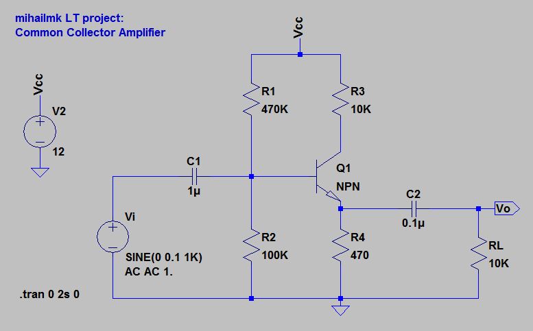
In the common collector amplifier circuit, the common electrode is the collector of the transistor, the input signal leads on the base and the output signal is taken from the emitter. The common collector circuit is shown on Picture 1. This is almost the same circuit configuration as the common emitter circuit that we already analyzed. The only difference here is the connection point of the load (with the output coupling capacitor C2) which is moved (reconnected) from the collector to the emitter of the transistor Q1. Here, again we will use the simplest circuit configuration.


Picture 1: Common Collector Amplifier Circuit


In general, the common collector amplifier circuit has relatively big input impedance and relatively small output impedance. The current amplification is usually big while the voltage amplification is close up to 1, but it's always less than 1. Because the output signal, which is taken from the emitter, is in phase with the input signal in the base of the transistor and it's close to it (since the voltage amplification is near to 1) we can say that the output follows the input. That's the reason why the common collector amplifier circuit is called "emitter follower". Using the simplified hybrid model for the transistor for common emitter circuit (He), the following simplified expressions for voltage and circuit amplification can be found:

Av = Vo/Vi = ( (1 + hfe)*(Re||Rl) ) / ( hie + (1 + hfe)*(Re||Rl) ) , --> for hfe >> 1 => Av ~ 1

Ai = Io/Ii = ( (1 + hfe) / ( 1 + (hie + (1 + hfe)*(Re||Rl))/Rth ) ) * ( Re/(Re + Rl) ) ,

where:

Re||Rl = (Re*Rl)/(Re+Rl) - parallel resistance of the emitter's resistance (Re, in our case R4) and load resistance (Rl);
Rth - is the equivalent Thévenin's resistance of the circuit, looking from its input - this equivalent resistance Rth is the resistance obtained at terminals A-B of the network with all its independent current sources open circuited and all its independent voltage sources short circuited - in our case terminal A is the input point of the circuit - electrode of the C1 and terminal B is the ground;


Time-domain analysis

The transient analysis of the circuit was performed as non-linear time-domain simulation for the first 2 seconds from applying the power supply and input signal. The time domain wave forms of the voltage signals of input and output are shown on the Picture 2. The blue color trace is the input voltage measured right before C1 (actually, that's the Vi waveform) and the green color trace is the output voltage measured right after the C2 (actually, that's the Vo waveform - the voltage of the load Rl). These wave forms are at time moment about 620 ms after the start of the simulation. As we can see from the Picture 2, the output signal is relatively ok, there are not any visible distortions of its wave form. Also, we can see that there is a little phase shift between input and output signals. Now, we can see more precise results from the simulation through the numbers measured in LT Spice (approximate values):

For Vi max = + 100 mV => Vo max = + 92,4 mV;
For Vi min = - 100 mV => Vo min = - 92,9 mV;

--> Av = 0.92 (approximate voltage amplification Av = Vo/Vi)

For Ic1 min = - 4.5 uA => IRl min = - 9.2 uA;
For IC1 max = + 15.7 uA => IRl max = + 9.2 uA;

--> Ai = 2 (approximate current amplification Ai = Io/Ii)

(*Ic1 is the current that flows through capacitor C1, and Irl is the current that flows through the load Rl)


Picture 2: Transient analysis - input and output voltage wave forms (time-domain)


So, according to numbers, min and max values of the output voltage signal vary for about 0.5 mV, which is not big value for the Vo amplitude of about 93 mV (about 0.5 % distortion). The approximate voltage amplification for this circuit configuration is about Av = 0.92, while the approximate current amplification is Ai = 2. Here, we have a big distortion of the input current signal, namely, for the negative half-period of the input signal the input current reaches minimum value of - 4.5 uA, and for the positive half-period it reaches maximum value of + 15.7 uA, which results in sharp positive peaks in the waveform. This is caused by the relatively high voltage level of the input signal for this circuit configuration. The high input voltage level, allows the transistor to enter into the non-linear region for the positive half-period of the signal and that results in the distorted current signal on its input, which also reflects on the input current passing through the coupling capacitor C1. Interesting thing here is that this distortion of the current signal do not appears on the output (as we can see from the measured values of IRl = +/- 9.2 uA). So, the conclusion from this will be that our circuit configuration needs different values for the components, which will change the dynamic mode of operation of the transistor Q1 in order to keep it in the linear normal active region. Also, we can eliminate this input current distortion with no changing of the circuit components values, but only with decreasing the input voltage level of the signal generator Vi. For example, if we set the amplitude to 10 mV (which is 10 times reduction from the previous amplitude of 100 mV), we will get again voltage amplification close to 1 and current amplification of about 3 (with undistorted input current signal). Anyway, that's only a option which requires decreasing of the input voltage level, but not changing the other circuit parameters. Of course, there are many other ways to re-design this circuit depending on the wanted results.


Frequency-domain analysis

The phase-frequency characteristics of this common collector circuit were measured with AC analysis in LT spice. LT Spice computes the small signal AC behavior of the circuit linearized about its DC operating point. Again, in this AC simulation were used these parameters:

Type of Sweep: Octave;
Number of points per octave: 1;
Start Frequency: 20 Hz;
Stop Frequency: 10 MHz;


Picture 3: AC Analysis - output voltage [dB] and its phase [degrees] (frequency-domain)


The simulation results are shown on Picture 3. The solid green line on the graph represents the Vo[dB] and the dashed green line represents the phase of the Vo, both in frequency-domain. The maximum of the Vo is the -0.5 dB which is achieved for the frequencies above 10 kHz and phase in that cases is 0 degrees, which means that the output voltage is in phase with input voltage. Vo decreases for 3 dB (falls on -3.5 dB) at frequency of 160 Hz with phase of +46 degrees and group delay of 580 us. At frequency of 20 Hz, the magnitude of the output voltage Vo is -18.8 dB with phase of +97 degrees and group delay of 2.2 ms. Here is good to notice that for the frequency of 1 kHz, and that's it the frequency of the input signal that we used for transient analysis of the circuit, the phase of the output signal is phase shifted from the input for about +10 degrees. That explains why the voltage waveform of Vo on the Picture 2 is shifted to the left in a relation to the input voltage waveform Vi. However, a phase shifting of +10 degrees is not a big time interval (for 1 kHz the period is 1 ms, so, the time shift is about 0.027 ms), so we can say that the output is relatively in phase with the input, as it was expected for this "emitter follower" circuit configuration.

So, according to the results of the AC analysis of this circuit, the low frequency limit is fl = 160 Hz.

The reduction of the amplification at low frequencies is caused by the coupling capacitors C1 and C2, while the reduction at high frequencies is caused by the parasitic capacitances of the transistor and the parallel capacitances which reconnect the signal to the ground.

____________________________________________


Now, we can resume the simulation results of our three basic amplifier circuits with bipolar transistor:

1. CE (Common Emmiter) Amplifier circuit

- approximate voltage amplification Av = Vo/Vi: Av = - 10
- approximate current amplification Ai = Io/Ii: Ai = - 30
- low frequency limit is fl = 83 Hz

2. CB (Common Base) Amplifier circuit

- approximate voltage amplification Av = Vo/Vi: Av = 5
- approximate current amplification Ai = Io/Ii: Ai = 0.18
- low frequency limit is fl = 570 Hz


3. CC (Common Collector) Amplifier circuit

- approximate voltage amplification Av = Vo/Vi: Av = 0.92
- approximate current amplification Ai = Io/Ii: Ai = 2
- low frequency limit is fl = 160 Hz

Common Base Amplifier


In the common base amplifier circuit, the common electrode is the base of the transistor, the input signal leads on the emitter and the output signal is taken from the collector. The common base circuit is shown on Picture 1. This is almost the same circuit configuration as the common emitter circuit that we already analyzed. The only difference here is the connection point of the input AC signal (with the input coupling capacitor C1) which is moved (reconnected) from the base to the emitter of the transistor Q1. Here, again we will use the simplest circuit configuration.


Picture 1: Common Base Amplifier Circuit


In general, the common base amplifier circuit has relatively small input impedance and relatively big output impedance. The voltage amplification is usually big while the current amplification is close up to 1, but it's always less than 1. Using the simplified hybrid model for the transistor for common emitter circuit (He), the following simplified expressions for voltage and circuit amplification can be found:

Av = Vo/Vi = ( hfe/hie ) * ( Rc||Rl )

Ai = Io/Ii = ( hfe/(1 + hfe + hie/Re) ) * ( Rc/(Rc + Rl) ) , --> for hfe >> 1, Rc >> Rl => Ai ~ 1

So, this circuit doesn't shift the phase of the output signal in relation to the input signal. As we can see from the Picture 1, all the components values in the common base circuit used in the LT spice simulation are the same as for the common emitter circuit. I choose the same values in order to see the differences in the responses of this circuit configuration. Just to be clear, as for the common emitter circuit, and for this circuit too, we can choose the different values for the components in order to achieve the best performance characteristics of the circuit. But, that's other problem, and depends a lot on what do you want to get from the circuit that you design. Here, the goal is to see the basic principle of operation of these circuit configurations.


Time-domain analysis

The transient analysis of the circuit was performed as non-linear time-domain simulation for the first 2 seconds from applying the power supply and input signal. The time domain wave forms of the voltage signals of input and output are shown on the Picture 2. The blue color trace is the input voltage measured right before C1 (actually, that's the Vi waveform) and the green color trace is the output voltage measured right after the C2 (actually, that's the Vo waveform - the voltage of the load Rl). These wave forms are at time moment about 620 ms after the start of the simulation. As we can see from the Picture 2, the output signal is relatively ok, there are not any visible distortions of its waveform. Also, we can see that the input and output signals are not in phase. Now, we can see more precise results from the simulation through the numbers measured in LT Spice (approximate values):

For Vi max = + 100 mV => Vo max = + 514.9 mV;
For Vi min = - 100 mV => Vo min = - 513.8 mV;

--> Av = 5 (approximate voltage amplification Av = Vo/Vi)

For Ic1 min = - 291 uA => IRl min = - 51 uA;
For IC1 max = + 291 uA => IRl max = + 51 uA;

--> Ai = 0.18 (approximate current amplification Ai = Io/Ii)

(*Ic1 is the current that flows through capacitor C1, and Irl is the current that flows through the load Rl)


Picture 2: Transient analysis - input and output voltage wave forms (time-domain)


So, according to numbers, min and max values of the output voltage signal vary for about 1 mV, which is not big value for the Vo amplitude of about 515 mV (about 0.2 % distortion). The approximate voltage amplification for this circuit configuration is about Av = 5, while the approximate current amplification is Ai = 0.18. So, Ai is less than 1, but it's not close to 1. That means that for our selected values of this circuit components we have relatively a big current attenuation (about 5, or Ii = 5 * Io), but with other values we can achieve a current amplification close to 1, if that's it what we want to achieve.


Frequency-domain analysis

The phase-frequency characteristics of this common base circuit were measured with AC analysis in LT spice. LT Spice computes the small signal AC behavior of the circuit linearized about its DC operating point. Again, in this AC simulation were used these parameters:

Type of Sweep: Octave;
Number of points per octave: 1;
Start Frequency: 20 Hz;
Stop Frequency: 10 MHz;


Picture 3: AC Analysis - output voltage [dB] and its phase [degrees] (frequency-domain)


The simulation results are shown on Picture 3. The solid green line on the graph represents the Vo[dB] and the dashed green line represents the phase of the Vo, both in frequency-domain. The maximum of the Vo is the 15.4 dB which is achieved for the frequencies above 10 kHz and phase in that cases is 0 degrees, which means that the output voltage is in phase with input voltage. Vo decreases for 3 dB (falls on 12.4 dB) at frequency of 570 Hz with phase of +52 degrees and group delay of 200 us. At frequency of 20 Hz, the magnitude of the output voltage Vo is -24.7 dB with phase of +163 degrees and group delay of 2.2 ms. Here is good to notice that for the frequency of 1 kHz, and that's it the frequency of the input signal that we used for transient analysis of the circuit, the phase of the output signal is phase shifted from the input for about +40 degrees. That explains why the voltage waveform of Vo on the Picture 2 is shifted to the left in a relation to the input voltage waveform Vi. The positive phase of +40 degrees, means a time shifting to left for about 1/9 of the period of the sinusoidal waveform (for 1 kHz the period is 1 ms, so the time shift is about 0.11 ms). That can be noticed on the Picture 2 if you look at the positive or negative peaks of the signals Vi and Vo (the Vo peaks are shifted to the left for about 0.11 ms in a relation to the Vi peaks).

So, according to the results of the AC analysis of this circuit, the low frequency limit is fl = 570 Hz.

The reduction of the amplification at low frequencies is caused by the coupling capacitors C1 and C2, while the reduction at high frequencies is caused by the parasitic capacitances of the transistor and the parallel capacitances which reconnect the signal to the ground.

Common Emitter Amplifier


One of the three base amplifier circuits with bipolar transistor is the circuit with common emitter. In this circuit, the common electrode is the emitter of the transistor, the input signal leads on the base and the output signal is taken from the collector. The common emitter circuit is shown on Picture 1. This is the simplest circuit configuration only with base elements for proper polarization of the transistor and with input signal generator and output load for simple analysis of the circuit. Actually, as shown on Picture 1, this is LT spice project. The goal here is to see the basic characteristics of the common emitter circuit and to see the possibilities that the powerful LT spice simulator provides. So, we will not use here a deep math analysis of the circuit and it's elements, since the LT spice is doing that for us. However, our goal here is to analyze the basic principles of this circuit, and to see how the basic parameters affect the circuit response.

First, let's see which are the basic elements for the proper work of this circuit. The power supply Vcc is the DC voltage source. Vcc provides static mode of work of this circuit. The resistors R1 and R2 are there to provide the proper polarization of the base of the transistor Q1, the proper "Bias Voltage". Here, the transistor Q1 is a bipolar transistor with NPN polarization. The resistor R3 is collector's resistor (it can be marked as Rc) and the resistor R4 is emitter's resistor (it can be marked as Re). That's all we need for the static mode (DC) of work. Now comes Ac mode. We have AC input voltage signal Vi which should be amplified passing through this circuit as output voltage signal Vo. Just to be clear, Vi and Vo are voltages, however, we can consider the input signal as current Ii, then the output will be considered as output current signal Io. The AC signals are passing through the capacitors C1 and C2. The input signal is provided by the sinusoidal voltage source, and it leads to the base of the Q1 through the C1. The amplified output signal is taken from the collector of the Q1, and it leads to the load Rl through the C2.


Picture 1: Common Emitter Amplifier Circuit


The response of the circuit (and all characteristics) depends on the values of all parameters, like voltage supply, resistors and capacitors values and of course, the amplifier element itself - the transistor Q1. Depending on the selected model of transistor, we should choose the proper values for the voltage supply, resistors and capacitors, in order to achieve the desired response of the circuit. The selected values of the circuit components will define the static working point of the circuit. Adjusting their values, we actually adjust the static working point of the transistor. If we want to get the maximum undistorted amplified signal on the output of the circuit, we should adjust the biasing point to the value which will provide work of the transistor only in its active region. The result will be that the transistor is always operating halfway between its cut-off and saturation regions, thereby allowing the transistor amplifier to accurately reproduce the positive and negative halves of any AC input signal superimposed upon the DC biasing voltage. In other cases, the output of the circuit will be distorted. The common emitter amplifier configuration using an NPN transistor has many applications, but is commonly used in audio circuits such as pre-amplifier and power amplifier stages. Getting the undistorted amplified signal on the output is so important in audio applications.

Anyway, here we will not go that deep in the analysis. Therefore, I choose some "casual" values of the components just to see the simulation results. For the transistor Q1 is used the basic NPN bipolar model from LT Spice library. This model is ideal bipolar NPN transistor. The DC power supply is Vcc = 12 V. The values of the resistors for bias voltage are R1 = 470K (kilo ohms) and R2 = 100K. The collector's resistor is R3 = 10K and the emitter's resistor is R4 = 470 ohms. The capacitors are C1 = 1uF (uF = micro Farad) and C2 = 0.1 uF. The load resistor is Rl = 10K. The input signal is provided by the AC voltage source with sinusoidal waveform Vi. The amplitude of the Vi is 100 mV, the frequency is f = 1 kHz and the DC offset is 0 V.


Time-domain analysis

First, the transient analysis simulation is done. The transient analysis of the circuit was performed as non-linear time-domain simulation for the first 2 seconds from applying the power supply and input signal. The time domain wave forms of the voltage signals of input and output are shown on the Picture 2. The blue color trace is the input voltage measured right before C1 (actually, that's the Vi waveform) and the green color trace is the output voltage measured right after the C2 (actually, that's the Vo waveform - the voltage of the load Rl). These waveforms are at time moment about 620 ms after the start of the simulation. As we can see from the Picture 2, the output signal is relatively ok, there are not any visible distortions of its waveform. The amplitude of the output signal is about 1 V, which means that with this circuit configuration we achieved a voltage amplification of Av = - 10. Well, if you asked yourself why the amplification has a negative value, that's because this circuit acts like phase inverter of the signal. In other words, when the input signal has positive value, the output signal has negative value, and vice versa, when input has negative value the output has positive value. This is also visible on the time-domain wave forms on the Picture 2 (when input signal has positive peak, the output signal has negative peak, and vice versa). So, these are the visible results from the plot. Now, we can see more precise results from the simulation through the numbers measured in LT Spice (approximate values):

For Vi max = + 100 mV => Vo min = - 993,830 mV;
For Vi min = - 100 mV => Vo max = + 989,596 mV;

--> Av = - 10 (approximate voltage amplification Av = Vo/Vi)

For Ic1 min = - 3.2 uA => IRl max = + 99.1 uA;
For IC1 max = + 3.6 uA => IRl min = - 99.3 uA;

--> Ai = - 30 (approximate current amplification Ai = Io/Ii)

(*Ic1 is the current that flows through capacitor C1, and Irl is the current that flows through the load Rl)


Picture 2: Transient analysis - input and output voltage wave forms (time-domain)


The minimum value of the Vo measured is bigger than maximum for about 4 mV, which is not a very big distortion for a 1V amplitude sinusoidal signal (about 0.4 % distortion). This means that when positive half period is present in the output signal, The transistor reach its limit of the normal active region a little bit faster than when negative half-period is present, and it can't reach the same max value as for negative half-period, but the difference is small, so we can say that the static mode of operation of this circuit is relatively well adjusted (for AC small signals with amplitudes up to 100 mV). Also, from the values that we got from the simulation results for this common emitter circuit configuration the calculated values for amplification are about Av = - 10 (for voltage) and Ai = - 30 (for current).


The amplification

The voltage amplification Av is defined as ratio between the output and input voltage Av = Vo/Vi.
The current amplification Ai is defined as ratio between the output and input current Ai = Io/Ii.

In most practical cases, especially for the initial behavioral assessment of the transistors amplifiers, can be applied a simplified model for the transistor taking into account only two of the h-parameters: hie and hfe, so allowing error no greater than 10% for voltage and circuit amplification can be found following simplified expressions:

Av = Vo/Vi = - (hfe/hie)*(Rc||Rl)

Ai = Io/Ii = (Vo/Rl)/(Vi/Ri) ,

where:

hfe - the current gain of the transistor;
hie - the input impedance of the transistor (corresponding to the base resistance);
Rc||Rl = (Rc*Rl)/(Rc+Rl) - parallel resistance of the collector's resistance (Rc, in our case R3) and load resistance (Rl);
Ri - input impendance of the circuit (Ri = Rth||hie, where Rth is the equivalent Thévenin's resistance of the circuit, looking from its input - this equivalent resistance Rth is the resistance obtained at terminals A-B of the network with all its independent current sources open circuited and all its independent voltage sources short circuited - in our case terminal A is the input point of the circuit - electrode of the C1 and terminal B is the ground);

The amplification depends on the frequency of the input signal. That dependence can be expressed as:

A = A(jw), where j is imaginary unit and w is circular frequency w = 2*Pi*f (Pi = 3.14)

At low and high frequencies the amplification is less than the amplification Ao at middle frequencies. The frequencies where it falls to value 0.707 (or, it decreases for 3 dB) from the value at middle frequencies, are called lower (fL) and upper (fH) frequency limits.


Frequency-domain analysis

The phase-frequency characteristics of this common emitter circuit were measured with AC analysis in LT spice. LT Spice computes the small signal AC behavior of the circuit linearized about its DC operating point. In this AC simulation were used these parameters:

Type of Sweep: Octave;
Number of points per octave: 1;
Start Frequency: 20 Hz;
Stop Frequency: 10 MHz;


Picture 3: AC Analysis - output voltage [dB] and its phase [degrees] (frequency-domain)


The simulation results are shown on Picture 3. The solid green line on the graph represents the Vo[dB] and the dashed green line represents the phase of the Vo, both in frequency-domain. The maximum of the Vo is the 20 dB which is achieved for the frequencies above 10 kHz and phase in that cases is -180 degrees. Vo decreases for 3 dB (falls on 17 dB) at frequency of 83 Hz with phase of -132 degrees and group delay of 1.2 ms. At frequency of 20 Hz, the magnitude of the output voltage Vo is 7.5 dB with phase of -90 degrees and group delay of 3.1 ms.

So, according to the results of the AC analysis of this circuit, the low frequency limit is fl = 83 Hz. Also, there is no high frequency limit for this circuit and that's because we used ideal model of transistor in this simulation. If we choose a real model transistor, then the output voltage/amplification will declines and for high frequencies too.

The reduction of the amplification at low frequencies is caused by the coupling capacitors C1 and C2, while the reduction at high frequencies is caused by the parasitic capacitances of the transistor and the parallel capacitances which reconnect the signal to the ground. At high frequencies special transistor models are used, like, for example, the Pi-hybrid model of transistor.

Netduino


Netduino is an open source electronics platform using the .NET Micro Framework. The .NET Micro Framework combines the ease of high-level coding and the features of microcontrollers. Featuring a 32-bit microcontroller and a rich development environment. Suitable for engineers and hobbyists alike.


Picture 1: Netduino 2


Technical specifications:

Processor and memory:

● STMicro 32-bit microcontroller;
● Speed: 120MHz, Cortex-M3;
● Code Storage: 192 KB;
● RAM: 60 KB.

Power:

● input: 7.5 - 9.0 VDC or USB powered;
● output: 5 VDC and 3.3 VDC regulated;
● max current: 25 mA per pin (microcontroller max current: est. 125 mA total);
● digital I/O are 3.3 V -- but 5 V tolerant.


Digital I/O features:

● all 22 digital and analog pins: GPIO;
● digital pins 0-1: UART 1 RX, TX;
● digital pins 2-3: UART 2 RX, TX/PWM;
● digital pins 5-6: PWM, PWM;
● digital pins 7-8: UART 3 RX, TX (also works as UART 2 RTS, CTS);
● digital pins 9-10: PWM, PWM;
● digital pins 11-13: PWM/MOSI, MISO, SPCK;
● digital pin SD/SC: SDA/SCL (also works as UART 4 RX, TX).


More information, downloads and support you can find at Netduino.


Source: Netduino.

Raspberry Pi


The Raspberry Pi is a credit-card sized computer that plugs into your TV and a keyboard. It is a capable little computer which can be used for many of the things that your desktop PC does, like spreadsheets, word-processing and games. It also plays high-definition video. We want to see it being used by kids all over the world to learn programming.


Picture 1: Raspberry Pi

Basic Features:

1. SD card
• Minimum size 4Gb; class 4 (the class indicates how fast the card is);
• We recommend using branded SD cards as they are more reliable.

2. HDMI to HDMI / DVI lead
• HDMI to HDMI lead (for HD TVs and monitors with HDMI input) or HDMI to DVI lead (for monitors with DVI input);
• Leads and adapters are available for few pounds -- there is no need to buy expensive ones.

3. RCA video lead
• A standard RCA composite video lead to connect to your analogue display if you are not using the HDMI output.

4. Keyboard and mouse
• Any standard USB keyboard and mouse should work;
• Keyboards or mice that take a lot of power from the USB ports, however, may need a powered USB hub. This may include some wireless devices.

5. Ethernet (network) cable [optional]
• Networking is optional, although it makes updating and getting new software for your Raspberry Pi much easier.

6. Power adapter
• A good quality, micro USB power supply that can provide at least 700mA at 5V is essential;
• Many mobile phone chargers are suitable—check the label on the plug;
• If your supply provides less than 5V then your Raspberry Pi may not work at all, or it may behave erratically. Be wary of very cheap chargers: some are not what they claim to be;
• It does not matter if your supply is rated at more than 700mA.

7. Audio lead [optional]
• If you are using HDMI then you will get digital audio via this;
• If you are using the analogue RCA connection, stereo audio is available from the 3.5mm jack next to the RCA connector.


More information about Raspberry Pi.


Source: Raspberry Pi Organization.

Arduino Uno


The Arduino Uno is a microcontroller board based on the ATmega328. It has 14 digital input/output pins (of which 6 can be used as PWM outputs), 6 analog inputs, a 16 MHz ceramic resonator, a USB connection, a power jack, an ICSP header, and a reset button. It contains everything needed to support the microcontroller; simply connect it to a computer with a USB cable or power it with a AC-to-DC adapter or battery to get started. The Uno differs from all preceding boards in that it does not use the FTDI USB-to-serial driver chip. Instead, it features the Atmega16U2 (Atmega8U2 up to version R2) programmed as a USB-to-serial converter.


Picture 1: Arduino Uno Board (front)


Specifications:


> Microcontroller: ATmega328;
> Operating Voltage: 5V;
> Input Voltage (recommended): 7-12 V;
> Input Voltage (limits): 6-20 V;
> Digital I/O Pins: 14 (of which 6 provide PWM output);
> Analog Input Pins: 6;
> DC Current per I/O Pin: 40 mA;
> DC Current for 3.3V Pin: 50 mA;
> Flash Memory: 32 KB (ATmega328) of which 0.5 KB used by bootloader;
> SRAM: 2 KB (ATmega328);
> EEPROM: 1 KB (ATmega328);
> Clock Speed: 16 MHz.


The Arduino Uno can be powered via the USB connection or with an external power supply. The power source is selected automatically. The Arduino Uno can be programmed with the Arduino software.


More information for Arduino Uno Board.


Source: ARDUINO.

Arduino Leonardo


The Arduino Leonardo is a microcontroller board based on the ATmega32u4. It has 20 digital input/output pins (of which 7 can be used as PWM outputs and 12 as analog inputs), a 16 MHz crystal oscillator, a micro USB connection, a power jack, an ICSP header, and a reset button. It contains everything needed to support the microcontroller; simply connect it to a computer with a USB cable or power it with a AC-to-DC adapter or battery to get started.
The Leonardo differs from all preceding boards in that the ATmega32u4 has built-in USB communication, eliminating the need for a secondary processor. This allows the Leonardo to appear to a connected computer as a mouse and keyboard, in addition to a virtual (CDC) serial / COM port. It also has other implications for the behavior of the board.


Picture 1: Arduino Leonardo Board (front)


Specifications:


> Microcontroller: ATmega32u4;
> Operating Voltage: 5V;
> Input Voltage (recommended): 7-12 V;
> Input Voltage (limits): 6-20 V;
> Digital I/O Pins: 20;
> PWM Channels: 7;
> Analog Input Channels: 12;
> DC Current per I/O Pin: 40 mA;
> DC Current for 3.3V Pin: 50 mA;
> Flash Memory: 32 KB (ATmega32u4) of which 4 KB used by bootloader;
> SRAM: 2.5 KB (ATmega32u4);
> EEPROM: 1 KB (ATmega32u4);
> Clock Speed: 16 MHz.


The Arduino Leonardo can be powered via the micro USB connection or with an external power supply. The power source is selected automatically. The Leonardo can be programmed with the Arduino software.


More information for Arduino Leonardo Board.


Source: ARDUINO.

Digitally-Enhanced Power Analog Control


Microchip's first Digitally-Enhanced Power Analog Product


Microchip introduced the MCP19111, the world’s first Digitally Enhanced Power Analog controller. Microchip’s Digitally-Enhanced Power Analog family combines the power and performance of an analog-based controller with the flexibility of a digital interface. These products maintain the fast and efficient analog feedback loop and incorporate a digital front-end. This digital front-end offers configurability, including the ability to include custom algorithms, as well as a communication interface.

Microchip also announced the expansion of its high-speed MOSFET family, with the new MCP87018, MCP87030, MCP87090 and MCP87130.

The MCP19111 Digitally Enhanced Power Analog family operates across a wide voltage range of 4.5 to 32V and offers a significant increase in flexibility over conventional analog-based solutions.


Picture 1: Microchip’s Expanding Power Solutions

The MCP19111, digital and analog power-management device, in combination with the expanded MCP87XXX family of high-speed MOSFETs, supports configurable, high-efficiency DC/DC power-conversion designs for a broad array of consumer and industrial applications.


For additional information visit Microchip’s site.


Source: Microchip.

Schneider Electric PowerLogic PM Power Meters


PowerLogic PM700 series power meter

The PM700 series meter offers outstanding quality, versatility, and functionality in a cost-effective, ultra-compact unit. The meter is simple to use and offers a large, bright LCD display for superior readability even in extreme lighting conditions and viewing angles. An ideal replacement for analog meters, PM700 meters can be used for stand-alone metering in custom panels, switchboards, switchgear, gensets, motor control centers, and UPS systems. Another series from Schneider Electric are PowerLogic PM800.


Picture 1: The PowerLogic PM700 Series Power Meter


Model PM710 Features

> Large Easy to Read Characters for viewing multiple values at one time to get a snapshot of your circuit;
> Basic Power Quality with true RMS electrical parameters up to the 15th harmonic;
> Sampling at 32 times per cycle;
> Communicates via RS-485 port (Modbus protocol for integration with energy management systems);
> 96x96mm design with a mounting depth of only 2 inches makes the power meter ideal for low voltage switchboards, shallow cable compartments,

standalone machines, and a wide range of commercial and industrial applications;
> No tools required. Mount meter with clips;
> ANSI C12.16 1.0 Accuracy Class.


Model PM750 Features

> All PM710 features;
> 2 digital inputs for status, alarms or demand input synchronization;
> 1 digital output for kWh-pulsing, alarm status, or external controlled output;
> 15 user configurable alarms;
> ANSI C12.20 0.5 Accuracy Class.


PowerLogic PM1200 series power meter

The PowerLogic PM1200 multifunction power meter provides all the basic features needed to monitor an electrical circuit affordably. It is made universal to avoid confusing part numbers and ordering information. Rugged enough to withstand industrial and commercial environments, this meter will help save on energy and installation costs, is easy to use, and adapts to various circuit requirements onsite. The PowerLogic PM1200 meter measures basic measurements (V, A, Hz & PF), energy, power, demand, THD and much more. These meters can be used for energy and power monitoring, demand monitoring, load studies and circuit optimization, energy balancing and optimization etc.

> Onsite configuration of CT and PT ratios and various other set points;
> Large and bright, 3-measurement alphanumeric LED display;
> Configurable analog load bar for at-a-glance check of load on feeders;
> Standard MODBUS output for remote monitoring and data logging.


PowerLogic PM5000 series power meter


Picture 2: The PowerLogic PM5000 Series Power Meter


The PowerLogic PM5000 series power meter is the new product line introduced in October 2013. This newest addition to the PowerLogic portfolio of power and energy meters is engineered on a compact and high performance platform. A range of models cover the full spectrum of buildings and industrial applications, within a wide range of value propositions. The highly-accurate, reliable meters are compliant with IEC 61557-12, IEC 62052/53 and IEC 61053-22 metering standards: PM5100 and PM5300 models are class 0.5S while PM5500 models are class 0.2S. Each meter in the PowerLogic PM5000 series offers combinations of features intended to fully complement the requirements of energy cost management applications. Essential features such as different communication and I/O options, a battery-backed real-time clock, alarms, multiple tariff schedules, MID compliance and data and event logging ensure the PM5000 series has the capabilities to perform energy cost allocation and tenant metering / sub-billing.


Each one of these power meters can be used in configuration like Measurement Circuit for 3-phase AC Power.


Source: Schneider Electric.

Siemens SIMEAS P Power Meter


SIMEAS P is a power meter for panel mounting with graphic display and background illumination. The major application area is power monitoring and recording at MV and LV level. The major information types are measured values, alarms and status information. Power monitoring systems with SIMEAS P, a permanently installed system, enables continuous logging of energy-related data and provides information on operational characteristics of electrical systems. SIMEAS P helps identify sources of energy consumption and time of peak consumption. This knowledge allows you to allocate and reduce energy costs.
Measured values include r.m.s values of voltages (phase-to-phase and/or phase-to-ground), currents, active, reactive and apparent power and energy, power factor, phase angle, harmonics of currents and voltages, total harmonic distortion per phase plus frequency and symmetry factor.

This digital power meter for panel mounting can be used in Measurement Circuit for 3-phase AC Power.


Picture 1: Siemens SIMEAS P Power Meter


The SIMEAS P comes with two binary outputs, which can be configured for energy pulses, limit violations or status signals. The unit is also able to trigger on settable limits. This function can be programmed for sampled or r.m.s. values. SIMEAS P generates a list of minimum, average and maximum values for currents, voltages, power, energy, etc. lndependent settings for currents, voltages, active and reactive power, power factor, etc. are also possible. In case of a violation of these limits, the unit generates alarms. Up to 6 alarm groups can be defined using AND/OR for logical combinations. The alarms can be used to increase counter values, to trigger the oscilloscope function, to generate binary output pulses, etc. The inputs and outputs of the Simeas P Power Meter are shown on Picture 2.


Picture 2: SIMEAS P Power Meter Inputs/Outputs


SIMEAS P Power Meter Features

> Measurement of voltage, current, active & reactive power, frequency, active & reactive energy, power factor, symmetry factor, voltage and current harmonics up to the 21st, total harmonic distortion;
> Single-phase, three-phase balanced or unbalanced connection, four-wire connection;
> PROFIBUS-DP orMODBUS RTU/ASCII or IEC 60870-5-103 communication protocol;
> Simple parameterization via front key or RS485 communication port using SIMEAS P PAR software;
> Graphic display with background illumination with up to 20 programmable screens;
> Battery: Recordings like limit value violations or energy counter values stay safely in the memory up to 3 months in case of a blackout;
> Real-time clock;
> 1 MB memory management: The allocation of the non-volatile measurement memory is programmable;
> Selectable screen types 2, 3, 4 or 6 measured values in one screen;
> One list screen for minimum, average and maximum values;
> Two types of screens for harmonics;
> One screen for oscilloscope function (sampled values or r.m.s. values);
> One screen serving as phasor (vector) diagram;
> Up to 20 screen types can be programmed. Switching from one screen to another can be automatic or manual.


Source: Siemens Energy.

KT77 Vacuum tube Pentode


The vacuum tube KT77 is the A.F. beam pentode tube. The dimensions and connections of the tube are shown on Picture 1. The following data are for the KT77 tube manufactured by JJ Electronic.


Picture 1: KT77 Vacuum Tube Pentode Dimensions and Connections


Electrical Data:

Cathode heater:

> Heater Voltage: 6.3 V;
> Heater Current: 1.4 A;

Typical Characteristics:

> Plate Voltage: 250 V;
> Screen Voltage: 250 V;
> Grid Voltage: -15 V;
> Plate Current: 100 mA;
> Screen Current: 10 mA;
> Transconductance: 10.5 mA/V;
> Amplification Factor: 11.5;

Limiting Values:

> Plate Voltage: 800 V max;
> Plate Dissipation: 25 W max;
> Screen Voltage: 800 V max;
> Screen Dissipation: 6 W max;
> Cathode Current: 180 mA max;
> Negative DC Grid Voltage: -200 V max.

Capacitances:

> Cg1 = 16.5 pF;
> Ca = 9 pF;
> Cag1 = 1 pF.


Source: JJ Electronic.

EL84 / 6BQ5 Vacuum tube Pentode


The vacuum tube EL84 or 6BQ5 is the R.F. output pentode tube. The dimensions and connections of the tube are shown on Picture 1. The following data are for the EL84 tube manufactured by JJ Electronic.


Picture 1: EL84 Vacuum Tube Pentode Dimensions and Connections


Electrical Data:

Cathode heater:

> Heater Voltage: 6.3 V;
> Heater Current: 760 mA;

Typical Characteristics:

> Plate Voltage: 250 V;
> Screen Voltage: 250 V;
> Grid Voltage: -7.3 V;
> Plate Current: 48 mA;
> Screen Current: 5.5 mA;
> Transconductance: 11.3 mA/V;
> Input Resistance: 40 kOhms;
> Amplification Factors (g1/g2): 19.

Limiting Values:

> Plate Voltage: 300 V max;
> Plate Dissipation: 12 W max;
> Screen Voltage: 300 V max;
> Screen Dissipation: 2 W max;
> Cathode Current: 65 mA max;
> Negative DC Grid Voltage: -100 V max.


Capacitances:

> Cgk = 10 pF;
> Cpk = 5.1 pF;
> Cgp = 0.6 pF.


Source: JJ Electronic.

ECC81 / 12AT7 Vacuum tube - Twin Triode


The vacuum tube ECC81 or 12AT7 is the double triode tube. The dimensions and connections of the tube are the same as for ECC83 tube. The following data are for the ECC81 tube manufactured by JJ Electronic.


Electrical Data:

Cathode heater:

> Heater Voltage Series/Parallel: 12.6/6.3 V;
> Heater Current Series/Parallel: 150/300 mA;

Typical Characteristics:

> Plate Voltage: 250 V;
> Grid Voltage: -2 V;
> Plate Current: 10 mA;
> Transconductance: 5.5 mA/V;
> Input Resistance: 11 kOhms;
> Amplification Factor: 60.

Limiting Values:

> Plate Voltage: 300 V max;
> Plate Dissipation: 2.5 W max;
> Cathode Current: 15 mA max;
> Negative DC Grid Voltage: -50 V max.


Source: JJ Electronic.

ECC82 / 12AU7 Vacuum tube - Twin Triode


The vacuum tube ECC82 or 12AU7 is the double triode tube. The dimensions and connections of the tube are the same as for ECC83 tube. The following data are for the ECC82 tube manufactured by JJ Electronic.


Electrical Data:

Cathode heater:

> Heater Voltage Series/Parallel: 12.6/6.3 V;
> Heater Current Series/Parallel: 150/300 mA;

Typical Characteristics:

> Plate Voltage: 250 V;
> Grid Voltage: -8.5 V;
> Plate Current: 10.5 mA;
> Transconductance: 2.2 mA/V;
> Input Resistance: 7.7 kOhms;
> Amplification Factor: 17.

Limiting Values:

> Plate Voltage: 300 V max;
> Plate Dissipation: 2.75 W max;
> Cathode Current: 20 mA max;
> Negative DC Grid Voltage: -50 V max;

Capacitances:

> Cgk = 1.9 pF;
> Cpk = 1.9 pF;
> Cgp = 1.63 pF.


Source: JJ Electronic.

ECC83 / 12AX7 Vacuum tube - Twin Triode


The most used triode in audio systems is ECC83 or 12AX7 twin triode. Here, we will show basic specification of the vacuum tube Sylvania 12AX7. On the Picture 1 is shown the vacuum tube ECC83 from JJ electronics and the base connections.


Picture 1: ECC83 (JJ) Vacuum Tube & Bottom view (base connections)


The Sylvania Type 12AX7 is a miniature high-mu twin triode having separate cathodes. This tube is designed for service as an audio voltage amplifier or phase inverter. The center tapped heater of the 12AX7 permits operation on both 12.6 or 6.3 V.


Mechanical Data:

> Bulb: T-6 1/2;
> Base: E9-1, Small Button 9-Pin;
> Outline: 6-2;
> Basing: 9A;
> Cathode: Coated Unipotential;
> Mounting Position: Any.


Electrical Data:

> Heater Voltage Series/Parallel: 12.6/6.3 V;
> Heater Current Series/Parallel: 150/300 mA;
> Heater-Cathode Voltage - Heater negative to Cathode: 200 V max (Total DC and Peak);
> Heater-Cathode Voltage - Heater positive to Cathode: 100 V max (DC);
> Heater-Cathode Voltage - Heater positive to Cathode: 200 V max (Total DC and Peak).


Ratings:

> Plate Voltage: 300 V max;
> Plate Dissipation: 1 W max;
> Positive DC Grid Voltage: 0 V max;
> Negative DC Grid Voltage: -50 V max;


Characteristics and Typical Operation:

Class 1 Amplifier

> Plate Voltage: 250 V;
> Grid Voltage: -2 V;
> Plate Current: 1.2 mA;
> Plate Resistance: 62.5 kOhms;
> Amplification Factor: 100.


Source: Sylvania Electric Products Inc.

Svetlana EL34/6CA7 Vacuum Tube


Svetlana EL34/6CA7 High Performance Audio Power Pentode


The Svetlana™ EL34 is a glass envelope power pentode having a plate dissipation rating of 25 Watts with convection cooling. It is intended for audio frequency power amplification service in either pentode, ultralinear or triode connection and single or push-pull/parallel applications. The Svetlana EL34 has an indirectly-heated oxide cathode, which may be DC operated for the absolute best hum/noise performance.

The Svetlana EL34 is manufactured with the original Mullard design in the Svetlana factory in St. Petersburg, Russia, and is designed to be a direct replacement for any EL34/6CA7 or equivalent. The Svetlana EL34 gives electrical and audio performance very similar to that of the original Mullard EL34.


Picture 1: Svetlana EL34/6CA7 Vacuum Tube & Bottom view (octal base connections)


Electrical Characteristics:


> Heater Voltage (AC or DC): Min. 5.7 V, Nom. 6.3 V, Max. 6.9 V
> Heater Current: 1.6 A
> Cathode: Oxide-coated, unipotential
> Cathode-to-heater potential, max. 100 V
> Direct interelectrode capacitances, max.:
- Grid no.1 to cathode and grid no.3, grid no.2, base sleeve and heater < 16 pF - Plate to cathode and grid no.3, grid no.2, base sleeve and heater < 0.6 pF - Grid no.1 to plate < 1.1 pF


Typical Operation - AF Power Amplifier, Class A1 (single tube):

> Plate Voltage 250 V
> Grid 2 Screen Voltage 250 V
> Grid 1 Control Voltage -14 V
> Peak AF Grid 1 Control Voltage 14 V
> Zero Signal Plate Current 100 mA
> Maximum Signal Plate Current 105 mA
> Zero Signal Grid 2 Screen Current (avg) 15 mA
> Transconductance (nominal) 11,000 µS
> Load Resistance 2000 Ohms
> Output Power at 5% distortion 10 W


*This tube can be find as SED EL34.


Source: Svetlana Tubes (SED Thermionic Valves).

The Only 0.8V/0.6µA Rail-To-Rail OP Amp

Touchstone Semiconductor has the world’s only family of < 1V, < 1µA Single, Dual, and Quad Op Amps.


About Single OP Amp TS1001 from Touchstone Semiconductor

The TS1001 is the industry’s first sub-1µA supply current, precision CMOS operational amplifier rated to operate at a nominal supply voltage of 0.8V. Optimized for ultra-long-life battery-powered applications, the TS1001 is Touchstone’s first operational amplifier in the “NanoWatt Analog™” high-performance analog integrated circuits portfolio. The TS1001 exhibits a typical input offset voltage of 0.5mV, a typical input bias current of 25pA, and rail-to-rail input and output stages. The TS1001 can operate from single-supply voltages from 0.65V to 2.5V.


Single OP Amp
Part Number: TS1001; Number of Amps: 1; Idd (max) = 1 µA; Package: SC70-5;

Dual OP Amp
Part Number: TS1002; Number of Amps: 2; Idd (max) = 2 µA; Package: MSOP-8;

Quad OP Amp
Part Number: TS1004; Number of Amps: 4; Idd (max) = 4 µA; Package: TSSOP-14;


Features:

VDD (min): 0.8 V;
VDD (max): 2.5 V;
GBW (kHz): 4;
Slew Rate (V/ms): 1.5;
Rail-to-Rail In/Out: Yes/Yes;
VOS (max): 3 mV;


Applications:

Battery/Solar-Powered Instrumentation
Portable Gas Monitors
Low-voltage Signal Processing
Nanopower Active Filters
Wireless Remote Sensors
Battery-powered Industrial Sensors
Active RFID Readers
Powerline or Battery Current Sensing
Handheld/Portable POS Terminals


Source: Touchstone Semiconductor.

IEC 11 or VDE D Group of coupling of 3-phase transformers


Picture 1: IEC 11 or VDE D Group of couplings of 3-phase transformers


On Picture 1 are shown the 3 types of coupling of three-phase transformers. According to IEC standard, this group of couplings is defined as Group 11, while according to VDE standard this same group of couplings is defined as Group D. The vector diagrams and the connection schematics are also shown on the figure for both, primary and secondary voltages or high and low voltages. The phase shifting per phase between the secondary and primary coils for this group is 330 degrees or 11 hours (according to the IEC standard this is represented as distance expressed in hours between the clock arrow for hours and the clock arrow for minutes which is always at fixed position at 12).

So, according to these standards this Group of couplings consists three couplings marked as:

1. Dy11 (IEC) or D1 (VDE);
2. Yd11 (IEC) or D2 (VDE);
3. Yz11 (IEC) or D3 (VDE);


As we can see, the IEC marking for the couplings is more descriptive than the VDE marking, since the mark actually represent the primary and secondary coupling connection and the number represents the phase shifting between them. So, the Dy11 coupling means delta-star connection with 330 degrees (11 hours) phase shift between secondary and primary voltage per phase, Yd11 is star-delta connection and Yz11 is star-zickzak connection.

In practice, there is a common need for two transformers working in parallel connection on the same network. One of the conditions for this parallel working is that secondary voltages per each phase must be in phase (no time delays) between the transformers. However, for this time synchronization between same phases from the two transformers it is not required the both transformers to have the same coupling. According to this, the transformers which belongs to the same group of couplings may work in parallel, of course, if the other conditions are also satisfied. So, two transformers which has any of the IEC Group 11 or VDE Group D coupling can work in parallel.

IEC 5 or VDE C Group of coupling of 3-phase transformers


Picture 1: IEC 5 or VDE C Group of couplings of 3-phase transformers


On Picture 1 are shown the 3 types of coupling of three-phase transformers. According to IEC standard, this group of couplings is defined as Group 5, while according to VDE standard this same group of couplings is defined as Group C. The vector diagrams and the connection schematics are also shown on the figure for both, primary and secondary voltages or high and low voltages. The phase shifting per phase between the secondary and primary coils for this group is 150 degrees or 5 hours (according to the IEC standard this is represented as distance expressed in hours between the clock arrow for hours and the clock arrow for minutes which is always at fixed position at 12).

So, according to these standards this Group of couplings consists three couplings marked as:

1. Dy5 (IEC) or C1 (VDE);
2. Yd5 (IEC) or C2 (VDE);
3. Yz5 (IEC) or C3 (VDE);


As we can see, the IEC marking for the couplings is more descriptive than the VDE marking, since the mark actually represent the primary and secondary coupling connection and the number represents the phase shifting between them. So, the Dy5 coupling means delta-star connection with 150 degrees (5 hours) phase shift between secondary and primary voltage per phase, Yd5 is star-delta connection and Yz5 is star-zickzak connection.

In practice, there is a common need for two transformers working in parallel connection on the same network. One of the conditions for this parallel working is that secondary voltages per each phase must be in phase (no time delays) between the transformers. However, for this time synchronization between same phases from the two transformers it is not required the both transformers to have the same coupling. According to this, the transformers which belongs to the same group of couplings may work in parallel, of course, if the other conditions are also satisfied. So, two transformers which has any of the IEC Group 5 or VDE Group C coupling can work in parallel.