Analog Inputs and Outputs


Many PLC-s also work with analog I/O devices. Analog devices use signals that are continuously variable within a specified range, such as 0 to 10 V DC or 4 to 20 mA. Analog signals are used to represent variable values, such as speed, rate of flow, temperature, weight, level, etc. In order to process an input of this type, a PLC must convert the analog signal to a digital value. Digital values from analog inputs are stored in addressable memory for use by the user program. Similarly, the user program can place digital values in addressable memory locations for conversion to analog values for the designated analog outputs.
Analog I/O points can be added using expansion modules for any CPU. The number of expansion modules depends on the CPU type and how many modules it can support. Expansion modules are available with 4 or 8 analog inputs, 2 or 4 analog outputs, or 4 analog inputs and 1 analog output (Or many other combinations, depending on the manufacturer and types). In addition, expansion modules are available for use with thermo-couples or RTD type sensors which sense the temperature at a specific point in a machine or process.


Analog Input Example


Analog inputs can be used for a variety of purposes. In the following example (Picture 1), a scale is connected to a load cell. A load cell is a device that generates an electrical output proportional to the force applied.


Picture 1: Analog Input Example


The load cell in this example converts a value of weight from 0 to 50 pounds into a 0 - 10 V DC analog value. The 0 - 10 V DC load cell signal is connected to an PLC’s analog input. The analog value applied to the PLC can be used in various ways. For instance, the actual weight can be compared to a desired weight for a package. Then, as the package is moved on a conveyor, the PLC can control a gate to direct packages of varying weight.


Analog Output Example


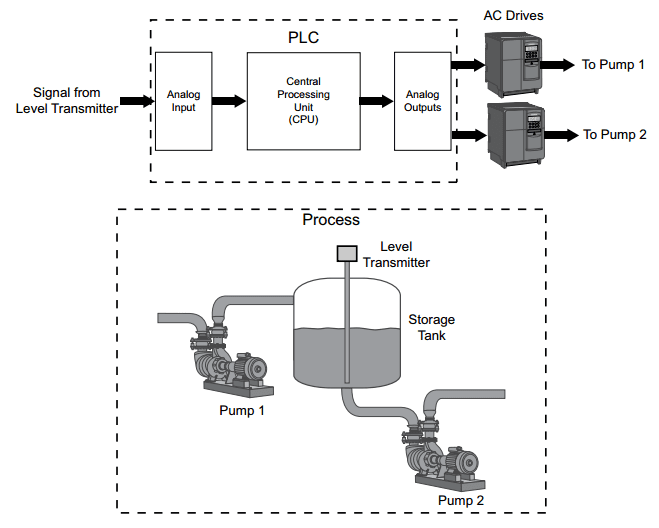
Analog outputs from a PLC are often supplied directly or through signal converters or transmitters to control valves, instruments, electronic drives or other control devices which respond to analog signals. For example, analog outputs from the PLC could be used to control the flow of fluid in a process by controlling AC drives (Picture 2). Rather than simply turning the AC drives on or off, which could be accomplished by discrete outputs, analog signals can be used to control the output of the AC drives. This would allow the speed of the pumps to be varied dynamically in response to changes in process requirements.


Picture 2: Analog Output Example

Discrete Inputs/Outputs


Motor Starter Example


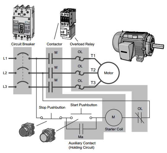
A more practical, and only slightly more complex application is start-stop control of an AC motor. Before examining the PLC application, first consider a hardwired approach. The following line diagram (Picture 1) illustrates how a normally open and a normally closed push button might be connected to control a three-phase AC motor. In this example, a motor starter coil (M) is wired in series with a normally open, momentary Start push button, a normally closed, momentary Stop push button, and normally closed overload relay (OL) contacts.


Picture 1: Motor Starter Example


Momentarily pressing the Start push button completes the path for current flow and energizes the motor starter (M). This closes the associated M and Ma (auxiliary contact located in the motor starter) contacts. When the Start button is released, current continues to flow through the Stop button and the Ma contact, and the M coil remains energized.
The motor will run until the normally closed Stop button is pressed, unless the overload relay (OL) contacts open. When the Stop button is pressed, the path for current flow is interrupted, opening the associated M and Ma contacts, and the motor stops.


PLC Motor Control


This motor control application can also be accomplished with a PLC. In the following example (Picture 2), a normally open Start push button is wired to the first input (I0.0), a normally closed Stop push button is wired to the second input (I0.1), and normally closed overload relay contacts (part of the motor starter) are connected to the third input (I0.2). These inputs are used to control normally open contacts in a line of ladder logic programmed into the PLC.


Picture 2: PLC Motor Control


Initially, I0.1 status bit is a logic 1 because the normally closed (NC) Stop push button is closed. I0.2 status bit is a logic 1 because the normally closed (NC) overload relay (OL) contacts are closed. I0.0 status bit is a logic 0, however, because the normally open Start push button has not been pressed. Normally open output Q0.0 contact is also programmed on Network 1 as a sealing contact. With this simple network, energizing output coil Q0.0 is required to turn on the motor.


Program Operation


When the Start push button is pressed, the CPU receives a logic 1 from input I0.0. This causes the I0.0 contact to close. All three inputs are now a logic 1.
The CPU sends a logic 1 to output Q0.0. The motor starter is energized and the motor starts.
The output status bit for Q0.0 is now a 1. On the next scan, when normally open contact Q0.0 is solved, the contact will close and output Q0.0 will stay on even if the Start push button is released.
When the Stop push button is pressed, input I0.1 turns off, the I0.1 contact opens, output coil Q0.0 de-energizes, and the motor turns off.


Adding Run and Stop Light Indicators


The application can be easily expanded to include indicator lights for run and stop conditions. In this example (Picture 3), a RUN indicator light is connected to output Q0.1 and a STOP indicator light is connected to output Q0.2.
The ladder logic for this application includes normally open Q0.0 contact connected on Network 2 to output coil Q0.1 and normally closed Q0.0 contact connected on Network 3 to output coil Q0.2. When Q0.0 is off, the normally open Q0.0 contact on Network 2 is open and the RUN indicator off. At the same time, the normally closed Q0.0 contact is closed and the STOP indicator is on.


Picture 3: Run and Stop Indicator states


When the Start button is pressed, the PLC starts the motor. Output Q0.0 is now on. Normally open Q0.0 contact on Network 2 is now closed and the RUN indicator is on. At the same time, the normally closed Q0.0 contact on Network 3 is open and the STOP indicator light connected to output Q0.2 is off.


Further Expansion


The PLC program can be further expanded to accommodate a wide variety of commercial and industrial applications (Picture 4). Start/Stop push buttons, selector switches, indicator lights, and signaling columns can be added. Motor starters can be added for control of additional motors. Over-travel limit switches can be added along with proximity switches for sensing object position. Various types of relays can be added to expand the variety of devices being controlled. As needed, expansion modules can be added to further increase the I/O capability. The applications are only limited by the number of I/Os and amount of memory available for the PLC.


Picture 4: Expansion Elements

Basic Ladder Logic Symbols


PLC ladder logic consists of a commonly used set of symbols that represent instructions. Understanding these basic symbols is essential to understanding PLC operation.


Picture 1: NO/NC Contacts, Coil & Box


Contacts


One of the most confusing aspects of PLC programming for first-time users is the relationship between the device that controls a status bit and the programming function that uses a status bit. Two of the most common programming functions are the normally open (NO) contact and the normally closed (NC) contact (Picture 1). Symbolically, power flows through these contacts when they are closed. The normally open contact (NO) is closed when the input or output status bit controlling the contact is 1. The normally closed contact (NC) is closed when the input or output status bit controlling the contact is 0.


Coils


Coils represent relays that are energized when power flows to them (Picture 1). When a coil is energized, it causes a corresponding output to turn on by changing the state of the status bit controlling that output to 1. That same output status bit may be used to control normally open and normally closed contacts elsewhere in the program.


Boxes


Boxes represent various instructions or functions that are executed when power flows to the box (Picture 1). Typical box functions include timers, counters, and math operations.


Entering Elements


Control elements are entered in the ladder diagram by positioning the cursor and selecting the element from a list. In the following example shown on Picture 2 the cursor has been placed in the position to the right of I0.2. A coil was selected from a pulldown list and inserted in this position.


Picture 2: Entering Element in Ladder diagram


AND Operation


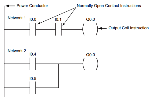
Each rung or network on a ladder represents a logic operation. The following programming example shown on Picture 3 demonstrates an AND operation. Two contact closures and one output coil are placed on network 1. They are assigned addresses I0.0, I0.1, and Q0.0. Note that in the statement list a new logic operation always begins with a load instruction (LD). In this example I0.0 (input 1) and (A in the statement list) I0.1 (input 2) must be true in order for output Q0.0 (output 1) to be true. This same logic is also shown in a function block diagram. The following truth table on Picture 3 represents the state of the output for each combination of input states.


Picture 3: AND Operation Ladder diagram


OR Operation


In this example (Picture 4), an OR operation is used in network 1. In the following example, if either input I0.2 (input 3) or (O in the statement list) input I0.3 (input 4), or both are true, then output Q0.1 (output 2) is true. The following truth table on Picture 4 represents the state of the output for each combination of input states.


Picture 4: OR Operation Ladder diagram

PLC Programming and Scan Process


Ladder Logic Programming


A program consists of instructions that accomplish specific tasks. The degree of complexity of a PLC program depends upon the complexity of the application, the number and type of input and output devices, and the types of instructions used. Ladder logic (LAD) is one programming language used with PLCs. Ladder logic incorporates programming functions that are graphically displayed to resemble symbols used in hard-wired control diagrams.
The left vertical line of a ladder logic diagram represents the power or energized conductor. The output coil instruction represents the neutral or return path of the circuit. The right vertical line, which represents the return path on a hard-wired control line diagram, is omitted. Ladder logic diagrams are read from left-to-right and top-to-bottom. Rungs are sometimes referred to as networks. A network may have several control elements, but only one output coil.


Picture 1: Ladder Logic Programming sample


Statement List and Function Block Diagrams


While ladder logic programs are still common, there are many other ways to program PLCs. Two other common examples are statement list and function block diagrams.
Statement list (STL) instructions include an operation and an operand. The operation to be performed is shown on the left. The operand, the item to be operated on, is shown on the right.
Function block diagrams (FBD) include rectangular functions with inputs shown on the left side of the rectangle and outputs shown on the right side.

In the following example (Picture 2), the program segments perform the same function.


Picture 2: STL, FBD, LAD samples


In addition to LAD, STL, and FBD, multiple other types of programming languages are used for PLCs. Each type of programming has its advantages and disadvantages. Factors such as application complexity, types of programming available for a specific PLC model, and user standards and preferences determine which type of programming is used for an application.


PLC Scan


The PLC program is executed as part of a repetitive process referred to as a scan. A PLC scan (Picture 3) starts with the CPU reading the status of inputs. Next, the application program is executed. Then, the CPU performs internal diagnostics and communication tasks. Finally, the CPU updates the status of outputs. This process repeats as long as the CPU in the run mode. The time required to complete a scan depends on the size of the program, the number of I/Os, and the amount of communication required.


Picture 3: PLC Scan Process

PLC-s


A programmable logic controller (PLC), also referred to as a programmable controller, is the name given to a type of computer commonly used in commercial and industrial control applications. PLC-s differ from office computers in the types of tasks that they perform and the hardware and software they require to perform these tasks. While the specific applications vary widely, all PLC-s monitor inputs and other variable values, make decisions based on a stored program, and control outputs to automate a process or machine.


Picture 1: PLC use


Basic PLC Operation


The basic elements of a PLC include input modules or points, a central processing unit (CPU), output modules or points, and a programming device (Picture 2). The type of input modules or points used by a PLC depends upon the types of input devices used. Some input modules or points respond to digital inputs, also called discrete inputs, which are either on or off. Other modules or inputs respond to analog signals. These analog signals represent machine or process conditions as a range of voltage or current values. The primary function of a PLC’s input circuitry is to convert the signals provided by these various switches and sensors into logic signals that can be used by the CPU.


Picture 2: Basic PLC Operation Elements


The CPU evaluates the status of inputs, outputs, and other variables as it executes a stored program. The CPU then sends signals to update the status of outputs. Output modules convert control signals from the CPU into digital or analog values that can be used to control various output devices.
The programming device is used to enter or change the PLC’s program or to monitor or change stored values. Once entered, the program and associated variables are stored in the CPU. In addition to these basic elements, a PLC system may also incorporate an operator interface device to simplify monitoring of the machine or process.

In the simple example shown below (Picture 3), push buttons (sensors) connected to PLC inputs are used to start and stop a motor connected to a PLC output through a motor starter (actuator). No programming device or operator interface are shown in this simple example.


Picture 3: Example - PLC in use of starting of motor


Hard-wired Control


Prior to PLC-s, many control tasks were performed by contactors, control relays, and other electro-mechanical devices. This is often referred to as hard-wired control. Circuit diagrams had to be designed, electrical components specified and installed, and wiring lists created (Picture 4). Electricians would then wire the components necessary to perform a specific task. If an error was made, the wires had to be reconnected correctly. A change in function or system expansion required extensive component changes and rewiring.


Picture 4: Hard-wired Control Circuit


Advantages of PLC-s


PLC-s not only are capable of performing the same tasks as hard-wired control, but are also capable of many more complex applications. In addition, the PLC program and electronic communication lines replace much of the interconnecting wires required by hard-wired control. Therefore, hard-wiring, though still required to connect field devices, is less intensive. This also makes correcting errors and modifying the application easier.

Some of the additional advantages of PLC-s are as follows:

• Smaller physical size than hard-wire solutions;
• Easier and faster to make changes;
• PLCs have integrated diagnostics and override functions;
• Diagnostics are centrally available;
• Applications can be immediately documented;
• Applications can be duplicated faster and less expensively.

The Sampling Theorem (Nyquist)


The definition of proper sampling is quite simple. Suppose you sample a continuous signal in some manner. If you can exactly reconstruct the analog signal from the samples, you must have done the sampling properly. Even if the sampled data appears confusing or incomplete, the key information has been captured if you can reverse the process.

Picture 1 shows several sinusoids before and after digitization. The continuous line represents the analog signal entering the ADC, while the square markers are the digital signal leaving the ADC. In (a), the analog signal is a constant DC value, a cosine wave of zero frequency. Since the analog signal is a series of straight lines between each of the samples, all of the information needed to reconstruct the analog signal is contained in the digital data. According to our definition, this is proper sampling.


Picture 1: Illustration of proper and improper sampling


The sine wave shown in (b) has a frequency of 0.09 of the sampling rate. This might represent, for example, a 90 cycle/second sine wave being sampled at 1000 samples/second. Expressed in another way, there are 11.1 samples taken over each complete cycle of the sinusoid. This situation is more complicated than the previous case, because the analog signal cannot be reconstructed by simply drawing straight lines between the data points. Do these samples properly represent the analog signal? The answer is yes, because no other sinusoid, or combination of sinusoids, will produce this pattern of samples (within the reasonable constraints listed below). These samples correspond to only one analog signal, and therefore the analog signal can be exactly reconstructed. Again, an instance of proper sampling.

In (c), the situation is made more difficult by increasing the sine wave's frequency to 0.31 of the sampling rate. This results in only 3.2 samples per sine wave cycle. Here the samples are so sparse that they don't even appear to follow the general trend of the analog signal. Do these samples properly represent the analog waveform? Again, the answer is yes, and for exactly the same reason. The samples are a unique representation of the analog signal. All of the information needed to reconstruct the continuous waveform is contained in the digital data. How you go about doing this will be discussed later in this chapter. Obviously, it must be more sophisticated than just drawing straight lines between the data points. As strange as it seems, this is proper sampling according to our definition.

In (d), the analog frequency is pushed even higher to 0.95 of the sampling rate, with a mere 1.05 samples per sine wave cycle. Do these samples properly represent the data? No, they don't! The samples represent a different sine wave from the one contained in the analog signal. In particular, the original sine wave of 0.95 frequency misrepresents itself as a sine wave of 0.05 frequency in the digital signal. This phenomenon of sinusoids changing frequency during sampling is called aliasing. Just as a criminal might take on an assumed name or identity (an alias), the sinusoid assumes another frequency that is not its own. Since the digital data is no longer uniquely related to a particular analog signal, an unambiguous reconstruction is impossible. There is nothing in the sampled data to suggest that the original analog signal had a frequency of 0.95 rather than 0.05. The sine wave has hidden its true identity completely; the perfect crime has been committed! According to our definition, this is an example of improper sampling.

This line of reasoning leads to a milestone in DSP, the sampling theorem. Frequently this is called the Shannon sampling theorem, or the Nyquist sampling theorem, after the authors of 1940s papers on the topic. The sampling theorem indicates that a continuous signal can be properly sampled, only if it does not contain frequency components above one-half of the sampling rate. For instance, a sampling rate of 2,000 samples/second requires the analog signal to be composed of frequencies below 1000 cycles/second. If frequencies above this limit are present in the signal, they will be aliased to frequencies between 0 and 1000 cycles/second, combining with whatever information that was legitimately there.


Two terms are widely used when discussing the sampling theorem: the Nyquist frequency and the Nyquist rate. Unfortunately, their meaning is not standardized. To understand this, consider an analog signal composed of frequencies between DC and 3 kHz. To properly digitize this signal it must be sampled at 6,000 samples/sec (6 kHz) or higher. Suppose we choose to sample at 8,000 samples/sec (8 kHz), allowing frequencies between DC and 4 kHz to be properly represented. In this situation there are four important frequencies: (1) the highest frequency in the signal, 3 kHz; (2) twice this frequency, 6 kHz; (3) the sampling rate, 8 kHz; and (4) one-half the sampling rate, 4 kHz. Which of these four is the Nyquist frequency and which is the Nyquist rate? It depends who you ask! All of the possible combinations are used. Fortunately, most authors are careful to define how they are using the terms. Here, they are both used to mean one-half the sampling rate.

Picture 2 shows how frequencies are changed during aliasing. The key point to remember is that a digital signal cannot contain frequencies above one-half the sampling rate (i.e., the Nyquist frequency/rate). When the frequency of the continuous wave is below the Nyquist rate, the frequency of the sampled data is a match. However, when the continuous signal's frequency is above the Nyquist rate, aliasing changes the frequency into something that can be represented in the sampled data. As shown by the zigzagging line in Picture 2, every continuous frequency above the Nyquist rate has a corresponding digital frequency between zero and one-half the sampling rate. If there happens to be a sinusoid already at this lower frequency, the aliased signal will add to it, resulting in a loss of information. Aliasing is a double curse; information can be lost about the higher and the lower frequency. Suppose you are given a digital signal containing a frequency of 0.2 of the sampling rate. If this signal were obtained by proper sampling, the original analog signal must have had a frequency of 0.2. If aliasing took place during sampling, the digital frequency of 0.2 could have come from any one of an infinite number of frequencies in the analog signal: 0.2, 0.8, 1.2, 1.8, 2.2, ... .


Picture 2: Conversion of analog frequency into digital frequency during sampling


Just as aliasing can change the frequency during sampling, it can also change the phase. For example, look back at the aliased signal in Picture 1 (d). The aliased digital signal is inverted from the original analog signal; one is a sine wave while the other is a negative sine wave. In other words, aliasing has changed the frequency and introduced a 180E phase shift. Only two phase shifts are possible: 0E (no phase shift) and 180E (inversion). The zero phase shift occurs for analog frequencies of 0 to 0.5, 1.0 to 1.5, 2.0 to 2.5, etc. An inverted phase occurs for analog frequencies of 0.5 to 1.0, 1.5 to 2.0, 2.5 to 3.0, and so on.

Now we will dive into a more detailed analysis of sampling and how aliasing occurs. Our overall goal is to understand what happens to the information when a signal is converted from a continuous to a discrete form. The problem is, these are very different things; one is a continuous waveform while the other is an array of numbers. This "apples-to-oranges" comparison makes the analysis very difficult. The solution is to introduce a theoretical concept called the impulse train.

Picture 3 (a) shows an example analog signal. Picture 3 (c) shows the signal sampled by using an impulse train. The impulse train is a continuous signal consisting of a series of narrow spikes (impulses) that match the original signal at the sampling instants. Each impulse is infinitesimally narrow. Between these sampling times the value of the waveform is zero. Keep in mind that the impulse train is a theoretical concept, not a waveform that can exist in an electronic circuit. Since both the original analog signal and the impulse train are continuous wave forms, we can make an "apples-apples" comparison between the two.


Picture 3: The sampling theorem in the time and frequency domains


Now we need to examine the relationship between the impulse train and the discrete signal (an array of numbers). This one is easy; in terms of information content, they are identical. If one is known, it is trivial to calculate the other. Think of these as different ends of a bridge crossing between the analog and digital worlds. This means we have achieved our overall goal once we understand the consequences of changing the waveform in Picture 3 (a) into the waveform in Picture 3 (c).

Three continuous wave forms are shown in the left-hand column in Picture 3. The corresponding frequency spectra of these signals are displayed in the right-hand column. This should be a familiar concept from your knowledge of electronics; every waveform can be viewed as being composed of sinusoids of varying amplitude and frequency. Later chapters will discuss the frequency domain in detail.

Picture 3 (a) shows an analog signal we wish to sample. As indicated by its frequency spectrum in (b), it is composed only of frequency components between 0 and about 0.33 fs, where fs is the sampling frequency we intend to use. For example, this might be a speech signal that has been filtered to remove all frequencies above 3.3 kHz. Correspondingly, fs would be 10 kHz (10,000 samples/second), our intended sampling rate.

Sampling the signal in (a) by using an impulse train produces the signal shown in (c), and its frequency spectrum shown in (d). This spectrum is a duplication of the spectrum of the original signal. Each multiple of the sampling frequency, fs, 2fs, 3fs, 4fs, etc., has received a copy and a left-for-right flipped copy of the original frequency spectrum. The copy is called the upper side-band, while the flipped copy is called the lower side-band. Sampling has generated new frequencies. Is this proper sampling? The answer is yes, because the signal in (c) can be transformed back into the signal in (a) by eliminating all frequencies above ½fs. That is, an analog low-pass filter will convert the impulse train, (b), back into the original analog signal, (a).

If you are already familiar with the basics of DSP, here is a more technical explanation of why this spectral duplication occurs. In the time domain, sampling is achieved by multiplying the original signal by an impulse train of unity amplitude spikes. The frequency spectrum of this unity amplitude impulse train is also a unity amplitude impulse train, with the spikes occurring at multiples of the sampling frequency, fs, 2fs, 3fs, 4fs, etc. When two time domain signals are multiplied, their frequency spectra are convolved. This results in the original spectrum being duplicated to the location of each spike in the impulse train's spectrum. Viewing the original signal as composed of both positive and negative frequencies accounts for the upper and lower side-bands, respectively. This is the same as amplitude modulation.

Picture 3 (e) shows an example of improper sampling, resulting from too low of sampling rate. The analog signal still contains frequencies up to 3.3 kHz, but the sampling rate has been lowered to 5 kHz. Notice that fs, 2fs, 3fs ... along the horizontal axis are spaced closer in (f) than in (d). The frequency spectrum, (f), shows the problem: the duplicated portions of the spectrum have invaded the band between zero and one-half of the sampling frequency. Although (f) shows these overlapping frequencies as retaining their separate identity, in actual practice they add together forming a single confused mess. Since there is no way to separate the overlapping frequencies, information is lost, and the original signal cannot be reconstructed. This overlap occurs when the analog signal contains frequencies greater than one-half the sampling rate, that is, we have proven the sampling theorem.

Alternate (2-way) Switch


The alternate or 2-way switch is basically a configuration of two switches which turn on or off the same load. This configuration is useful in many practice cases. The switches are placed on different physical locations, but they are both connected to the same load. A common use of this configuration can be found in our homes or buildings, mostly for switching on and off the light in some room, halls, stairs, etc.
For example, when we approach to the stairs for the next floor in our home, we want to turn on the light at the beginning of the stairs, and then to turn off the same light at the end, when we arrived at the top of them, and vice versa. In order to achieve this, we need to connect two switches which will power on/off the light. One switch will be placed at the bottom of the stairs, and the other at the top. These switches should be connected to each other in a way that when we turn on/off each one of them, they will bring the load to the opposite state of its current state. In other words, if the light is turned on, no matter which switch we will press now, the switch should turn off the light. After the light is turned off, again, no matter which switch we will press, it should turn on the light again, and so on.


Picture 1: Alternate 2-way Switch configuration diagram


So, in order to achieve this functionality, we need to connect the switches in a proper way. One configuration diagram for alternate switch is shown on Picture 1. As we can see from the picture, we have two switches SW1 and SW2 connected to each other and to the load, the light bulb. The switches in this configuration are 2-way switches, which have 3 connection terminals, marked as 1, 0 and 2. So, when the switch is in position 1, it has connection between the terminals 0 and 1, and when is in position 2, it has connection between the terminals 0 and 2. As shown on the diagram, the hot line from the power supply, the phase R, is connected to the terminal 2 of the switch SW1. Then, the terminals of the both switches are connected to each other: terminal 0 of SW1 is connected to the terminal 0 of SW2, terminal 1 of SW1 to the terminal 1 of SW2, and terminal 2 of SW1 to the terminal 2 of SW2. The hot terminal of the light bulb is connected to the terminal 1 of the second switch SW2, and the neutral line is connected directly to the light. The currently shown positions of the switches on Picture 1, provide the hot line to come to the bulb, so the light is turned on. In this state, the switch SW1 is in position 2 and the switch SW2 is in position 1. At this state, if we change the position of one of the switches, no matter which of them, we will cut the hot line path, and the light will turn off. After that, it's easy to see, that each next change in the position of the switches, no matter which of them, will altere the state of the light, turning it on and off, alternating. That's why we call this switch configuration an alternating switch. The configuration of the switches and connections seems to be simple, but the functionality is very practical and effective.

NanoPi Neo-Air


The NanoPi NEO Air is a 40 x 40mm open source ARM board for makers. It uses an Allwinner H3 Quad Core A7 processor at 1.2GHz. Its pins are compatible with the NanoPi NEO (V 1.2) and its 24-pin header is compatible with Raspberry Pi's GPIO pin headers. The NanoPi NEO AIR features 512MB of 16bit wide DDR3 RAM, 8GB eMMC and one MicroSD slot. It has WiFi & Bluetooth and DVP camera interface(YUV422). The DVP camera interface can support friendly arm's 5M-pixel camera module. It has enhanced power circuit design and better heat dissipation.


Picture 1: NanoPi NEO-Air Board layout


Features:


  • >> CPU: Allwinner H3, Quad-core Cortex-A7 Up to 1.2 GHz;
  • >> Memory: 512 MB DDR3 RAM;
  • >> Storage: 8 GB/32 GB eMMC;
  • >> WiFi: 802.11b/g/n;
  • >> Bluetooth: 4.0 dual mode;
  • >> MicroSD Slot x 1;
  • >> MicroUSB: OTG and power input;
  • >> DVP Camera interface: 0.5 mm pitch 24-pin FPC seat;
  • >> Debug Serial Port: 4Pin, 2.54 mm pitch pin header;
  • >> Audio Port: 4Pin, 2.54 mm pitch pin header;
  • >> GPIO1: 2.54 mm spacing 24 pin, includes UART, SPI, I2C, GPIO;
  • >> GPIO2: 2.54 mm spacing 12 pin, includes USB x2, IR, SPDIF, I2S;
  • >> PCB Size: 40 x 40 mm;
  • >> PCB layers: 6;
  • >> Power Supply: DC 5 V/ 2 A;
  • >> Weight: 7.5 g (without Pin-headers); 9.7 g (with Pin-headers);
  • >> Working Temperature: -40℃ to 80℃
  • >> OS/Software: u-boot, Ubuntu-Core-Xenial, Debian-Jessie;


More info: NanoPi.