Linear Amplifiers Class A, B and AB


Linear amplifiers, are amplifiers with a linear output stage, in which there exists a voltage drop across the output transistors to generate the correct output voltage. Even though most of these amplifiers use some sort of switching, they are not to be confused with switching amplifiers. The output stage of a power amplifier has perhaps the greatest influence on performance and cost. The output stage must also operate at high power levels, often at elevated temperatures, where difficult loads, high voltages, and high currents may exist. Indeed, there is often a trade-off between heat generation and sound quality.

Every real amplifier has some unavoidable limitations on its performance. Some of the main limitations which should be considered are:

>> Limited bandwidth. In particular, for each amplifier there will be an upper frequency beyond which it finds it difficult or impossible to amplify signals.
>> Noise. All electronic devices tend to add some random noise to the signals passing through them, degrading the SNR (signal-to-noise ratio).
>> Limited output voltage, current and power levels. This means that a given amplifier can't provide output signals above a particular level. In other words, there is always a finite limit to the output signal size.
>> Distortion. The actual signal pattern will be altered due to non-linearities in the amplifier.
>> Finite gain. A given amplifier can have a high gain, but this gain can't be infinite, so may not be large enough for a given purpose. That's why multiple amplifiers or stages are often used to achieve a desired overal gain.

The various limitations demands the various changes in the design of the amplifiers. That lead us to the concept of amplifier classes.


Class A, B and AB


The output transistors in a push-pull class A power amplifier remain in conduction throughout the entire cycle of the audio signal, always contributing transconductance to the output stage signal path. In contrast, the output transistors in a class B design remain on for only one-half of the signal cycle. When the output stage is sourcing current to the load, the top transistor is on. When the output stage is sinking current from the load, the bottom transistor is on. There is thus an abrupt transition from the top transistor to the bottom transistor as the output current goes through zero.
The formal definition of classes A and B is in terms of the so-called conduction angle. The conduction angle for class A is 360 degrees (meaning all of the cycle), while that for class B is 180 degrees. More accurately, the definition should really be the angle over which the transistor contributes transconductance to the output stage and signal current to the output. This precludes many so-called nonswitching amplifiers from being called class A. Such amplifiers include bias arrangements that prevent the power transistor from completely turning off when it otherwise would. Most power amplifiers are designed to have some overlap of conduction between the top and bottom output transistors. This smoothes out the crossover region as the output current goes through zero. For small output signal currents, the output transistors are in the overlap zone and the output stage effectively operates in class A. These amplifiers are called class AB amplifiers because they possess some of the characteristics and advantages of both class A amplifiers and class B amplifiers. Most push-pull vacuum tube amplifiers operate in class AB mode. Class AB output stages have a conduction angle that is greater than 180 degrees, although sometimes only slightly so.


Class A


A simple example of a Class A amplifier stage is a common emitter amplifier circuit. Class A amplifiers have the general property that the output device(s) always carry a significant current level, or they have a large quiescent current. The quiescent current is defined as the current level in the amplifier when it is producing an output of zero. The main disadvantage of Class A amplifiers is that current is flowing through the output transistor and its resistor even when there is no signal. Power is being used but no sound or other form of output activity occurs. Such amplifiers are inefficient because they waste 50% of the energy supplied to them. If an amplifier is to produce enough output power to drive a motor or high-wattage speaker, we must design the output stage of the circuit to avoid such waste. The most inefficient amplifier is single ended. More efficient amplifier can be made by employing a double ended or push-pull arrangement. On Picture 1 is shown an example of output stage in push-pull arrangement which works in Class A. This arrangement employs a pair of transistors, one is an NPN, the other is a PNP bipolar transistor.


Picture 1: Push-Pull output stage in Class A


The transistors in this circuit can be controlled using a pair of input voltages, V1 and V2. Therefore, the currents I1 and I2 can be altered independently, by wish. In practice, the easiest way to use the circuit is to set the quiescent current to half the maximum level we except to require for the load. Then adjust the two transistor currents "in oposition". It is the imbalance between the two transistor currents that will pass through the load, so this means the transistors "share" the burden of driving the output load.


Class B


Simply by changing the quiescent current or bias level in class A amplifier and then operating the system slightly differently, we can make another forms of amplifier. The simplest alternative is the Class B arrangement. To illustrate how this work, consider the circuit shown on Picture 2. This arrangement again employs a pair of transistors. However, their bases (or inputs) are now linked by a pair of diodes. The current in the diodes is mainly set by a couple of constant current stages which run a bias current, ibias, through them. If the forward voltage drop across each diode is Vd, then the voltage of the input to the base of the upper transistor is Vin + Vd, while the voltage of the input to the base of the lower transistor is Vin - Vd. Taking into account that the base-emitter junction of a bipolar transistor is essentially a diode, then the voltage drop between the base and the emitter of the transistors will also be Vd, by absolute value. That leads to the very interesting result where the emitter voltages in the circuit shown on Picture 2 will be V1 = V2 = Vin.


Picture 2: Class B output stage amplifier


This result has two implications. First, when Vin = 0, the output voltages will be zero. Since the voltages above and below the emitter resistors RE will both be zero, it follows that there will be no current at all in the output transistors. The quiescent current level is zero and the power dissipated when there is no output is also zero. So, this circuit has perfect efficiency. The second implication is that as Vin is adjusted to produce the signal, the emitter voltages will both tend to follow it. When the load is connected to the output circuit, it will draw current from one or the other transistor, but not from both. When a positive voltage is produced, the upper transistor conducts and draws the current through the load and the lower transistor is Off. On the ther hand, when a negative voltage is produced, the lower transistor conducts and draws the current through the load and the upper transistor is Off. This again means that the system is highly efficient in power terms.

When power efficiency is the main requirement, then Class B is very useful. However, for this circuit to work as explained, it requires the voltage drops across the diodes and the base-emitter junctions of the transistors to be exactly the same. In practice, this is impossible for many reasons. Firstly, no two physical devices are absolutely identical. The diodes and the transistors will have differently doped and manufactured junctions, designed for different purposes. The currents through the transistors is far higher then through the diodes. The transistors will be hotter than the diodes due to the higher power dissipation. When the applied voltage is changed, it takes a time for a PN junction to react and for the current to change. Also, the transistor can't be turned off right away and stop conducting. As a result, the transistors tend to lag behind any swift changes.

The overall result of the above effect is that the Class B arrangement tends to have difficulty whenever the signal waveform changes its polarity and the transistors turns on and off. The result is what is called crossover distortion and this have a very bad effect on small level or high speed waveforms. This problem is enhanced due to non-linearities in the transistors, meaning that the output current and voltage don't vary linearly with the input level. The effect of the crossover distortion is shown on Picture 3. It is proportionately greater in small signals.


Picture 3: Crossover distortion (as the signal swings between positive and negative)


So, the Class A is very power inefficient, while the Class B is far more efficient, but it can lead to signal distortions. The solution is to find a half-way which will take advantages of both arrangements and will minimize the problems. The most common solution is Class AB amplification.


Class AB


The Class AB arrangement can be seen to be very similar to the Class B circuit. In the example shown on Picture 4, it just has an extra pair of diodes. The change that these makes is, when there is no output, there is a potential difference of about 2 x Vd between the emitters of the transistors. As a consequence, there will be a quiescent current of about Iq = Vd/RE, flowing through both transistors when the output is zero. For small output signals (which requires output currents in the range -2Iq < IL < 2Iq), both transistors will conduct and act as a double ended Class A arrangement. For larger signals, one transistor will be off and the other will supply the current required by the load. Hence for large signals the circuit behaves like a Class B amplifier, this mixed mixed behaviour caused this arrangement to be called Class AB.


 Picture 4: Class AB output stage amplifier


Summary


Class A amplifiers employ a high quiescent or bias current, which causes large transistor currents even when the output signal level is small. Therefore, the power efficiency of class A amplifiers is poor, but they can offer good signal performance due to avoiding problems with effects due to low current level nonlinearities causing distortion. Double ended output design is more efficient than a single ended. Class B has a very low or perhaps zero quiescent (bias) current, and hence low power dissipation and optimum power efficiency. Class B may suffer from problems when handling low level signals. That's why the class AB is often the preferred solution in practice.

Amplifier Noise


Although the noise characteristics of a power amplifier are not as critical as those of a preamp, it is still important to achieve low noise because there is no volume control in the power amplifier to reduce noise from the input stage under normal listening conditions. This is particularly so when the amplifiers are used with high-efficiency loudspeakers. Power amplifier noise is usually specified as being so many dB down from either the maximum output power or with respect to 1 W. The former number will be larger by 20 dB for a 100 W amplifier, so it is often the one that manufacturers like to cite. The noise referenced to 1 W into 8 W (or, equivalently 2.83 V RMS) is the one more often measured by reviewers.
The noise specification may be unweighted or weighted. Unweighted noise for an audio power amplifier will typically be specified over a full 20 kHz bandwidth (or more). Weighted noise specifications take into account the ear’s sensitivity to noise in different parts of the frequency spectrum. The most common one used is A weighting, illustrated in Picture 1. Notice that the weighting curve is up about +1.2 dB at 2 kHz, whereas it is down 3 dB at approximately 500 Hz and 10 kHz.

The noise arising from different sources is usually assumed to be uncorrelated. For this reason, it adds on a power basis. This means that noise voltage adds up on an RMS basis as the square root of the sum of the squares of the various sources. Two noise sources each 10 µV RMS will add to 14.1 µV RMS. Two noise sources, one 10 µV and the other 3 µV will sum to 10.44 = µV. This shows how a larger noise source will tend to dominate over a smaller noise source.


Noise Bandwidth


Most noise sources have a flat noise spectral density, meaning that there is the same amount of noise power in each hertz of frequency spectrum. This means that total noise power in a measurement is proportional to the bandwidth of the measurement being made. This gives rise to the concept of noise bandwidth. A perfect brick-wall filter would have a noise bandwidth equal to its signal bandwidth. Because real filters roll-off gradually, the noise bandwidth is slightly different than the 3 dB bandwidth of a filter (often slightly more).


Noise Voltage Density


White noise has equal noise power in each hertz of bandwidth. If the number of hertz is doubled, the noise power will double, but the noise voltage will increase by only 3 dB or a factor of 2. Thus noise voltage increases as the square root of noise bandwidth, and noise voltage is expressed in nanovolts per root hertz nV/sqrt(Hz). There are 141 sqrt(Hz) in a 20 kHz bandwidth. A 100 nV/sqrt(Hz) noise source will produce 14.1 µV RMS in a 20 kHz measurement bandwidth.
As an aside, so-called pink noise has the same noise power in each octave of bandwidth. Pink noise is usually employed in certain test measurements. Pink noise is created by passing white noise through a low-pass filter having a 3 dB per octave roll-off slope.


A-Weighted Noise Specifications


The frequency response of the A-weighting curve is shown on Picture 1. It weights the noise in accordance with the human ear’s perception of noise loudness. The A-weighted noise specification for an amplifier will usually be quite a bit better than the unweighted noise because the A-weighted measurement tends to attenuate noise contributions at higher frequencies and hum contributions at lower frequencies. A very good amplifier might have an unweighted signal-to-noise ratio of –90 dB with respect to 1 W into 8 W, while that same amplifier might have an A-weighted SNR of 105 dB with respect to 1 W. The A-weighted number will sometimes be 10-20 dB better than the unweighted number.


Picture 1: A-weighting frequency response


Power Supply Noise


The power supply rails in any amplifier are often corrupted by numerous sources of noise. These may include random noise and other noises like power supply ripple and EMI and program-dependent noise from the output stage. The power supply noise can get into the signal path as a result of the signal circuit’s limited power supply rejection ratio (PSRR).
There are two important ways to control power supply noise. The first is to do a better job filtering the power supply rails. This is especially effective for power supply rails that provide power to low-level circuits. The second is to employ circuit topologies that have inherently high PSRR. The ability of a circuit to reject power supply noise usually decreases as the frequency of the noise increases. In other words, PSRR degrades at high frequencies. Fortunately, it is often possible to do a more effective job of filtering the power supply rails at higher frequencies.


Resistor Noise


All resistors have noise. This is referred to as Johnson noise or thermal noise. It is the most basic source of noise in electronic circuits. It is most often modeled as a noise voltage source in series with the resistor. The noise power in a resistor is dependent on temperature. It's determined as:

Pn = 4kTB [W]

k - Boltzman’s constant (k = 1.38 × 10^–23 J/°K);
T - temperature in °K (300°K @ 27°C);
B - bandwidth in hertz [Hz];

So, the resistor noise power density per Hertz, at temperature of 27°C (300°K) is pn = 1.66 × 10^–20 [W/Hz].

The open-circuit RMS noise voltage across a resistor of value R is simply:

en = sqrt(4kTRB)

or, en = 0.129 nV/sqrt(Hz) per sqrt(Ω) Noise voltage for a resistor thus increases as the square root of both bandwidth and resistance. A convenient reference is the noise voltage of a 1 kΩ resistor: 4.1 nV/sqrt(Hz). From this the noise voltage of any resistance in any noise bandwidth can be estimated.


BJT (Shot) Noise


Bipolar transistors generate a different kind of noise. This noise is related to current flow and the discreteness of current. This is called shot noise and is associated with the current flows in the collector and the base of the transistor. The collector shot noise current is usually referred back to the base as an equivalent input noise voltage in series with the base. It is referred back to the base as a voltage by dividing it by the transconductance of the transistor. Once again, the resulting input-referred noise is usually measured in nanovolts per root hertz.
The shot noise current is usually stated in picoamperes per root hertz [pA/sqrt(Hz)] and has the RMS value of:

Ishot = sqrt(2qIdcB)

q - 1.6 × 10^–19 Coulombs per electron;
B - bandwidth in Hertz;

It is easily seen that shot noise current increases as the square root of bandwidth and as the square root of current. An 1 mA collector current flow will have a shot noise component of 18 pA/sqrt(Hz).
The transconductance of a BJT operating at 1 mA is 38.5 mS. Dividing the shot noise current by gm we have input-referred noise en = 0.47 nV/sqrt(Hz). According to the equation for en, we can see that this is the voltage noise of a 13 Ω resistor. At the same time, notice that re’ for this transistor is 26 Ω. The noise voltage for a 26 Ω resistor is 0.66 nV/sqrt(Hz). The input-referred voltage noise of a transistor is equal to the Johnson noise of a resistor of half the value of re’. This is a very handy relationship.


JFET Noise


JFET noise results primarily from thermal channel noise. That noise is modeled as an equivalent input resistor rn whose resistance is equal to approximately 0.6/gm. If we model the effect of gm as rs’ (analogous to re’ for a BJT), we have rn = 0.6rs’. This is remarkably similar to the equivalent voltage noise source for a BJT, which is the voltage noise of a resistor whose value is re’/2. The noise of a BJT goes down as the square root of Ic because gm is proportional to Ic, and re’ goes down linearly as well. However, the gm of a JFET increases as the square root of Id. As a result, JFET input voltage noise goes down as the 1/4 power of Id.

An IEC Variant


The main problem with the IEC signal lies in its need for a noise source. Therefore, a new test signal is proposed that is equivalent to the IEC test signal. The noise source is replaced by 24 square waves of equal amplitude, all a factor 2 in frequency apart. In the frequency range from 10 Hz up to 28 kHz, this simulates pink noise, since the energy per octave is constant. This semi pink noise is filtered to get the IEC frequency characteristics. An additional advantage is that the signal, which had only 24 possible amplitude values, now becomes continuous. Only 100 ms of simulation with this IEC variant suffice, since frequency components below 10 Hz are not present. The square waves are easy to define in a circuit simulator, which will speed up simulations. Also, such a signal can easily be generated in hardware with binary counters or with IC’s that are used as tone generators in electronic organs. To see if this IEC variant is indeed equivalent, the dissipation curves for the three amplifier classes were measured, this time for the IEC signal and its variant. The results in Picture 1 show that the dissipations are almost the same at low output powers. At high output powers, the results differ more. Since heat sink temperature measurements on more than one high power music fragment are not available, it remains unclear if this error is the same for all music fragments at that output power. However, the differences are rather small and only occur when the signal is heavily clipping. At lower, more usual output powers, the IEC variant gives good results.


Picture 1: Measured dissipation of three amplifier classes for the IEC signal and the IEC variant

A Simple Periodic Test Signal


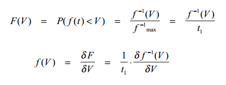
The IEC signal is suitable for measuring the efficiency of audio amplifiers, but for prediction purposes it is less ideal. The signal is difficult to generate when the efficiency of an amplifier has to be simulated in a circuit simulator. In circuit simulators, transient noise sources are rarely available, and usually take a long simulation time. Also, for long term testing (reliability), a noise generator is often not available. A simple, periodic test signal would be welcome. The most important quality is a controlled amplitude probability density function. Suppose the signal is V = f(t), and that it is monotonously rising on t∈ [0,t1]. The distribution function is the chance that f(t) is smaller than a certain value V, is:


Picture 1: The distribution function F(V) and The probability density function f(V)


As it can be seen from Picture 1, the probability density function f(V) is the derivative of the distribution function F(V). So if we want to design a signal with a gaussian amplitude probability density function, we know that f(V) is a gaussian curve. Then, f^-1(V) is the integral of a gaussian curve, which is the normal distribution function. Thus, f(t) must be the inverse of the normal distribution function. Picture 2 shows a possible time function.


Picture 2: Signal with a gaussian amplitude distribution


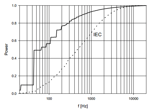
Picture 3: Frequency distribution of a signal with gaussian amplitude distribution (Picture 2), and of the IEC signal


Unfortunately, the corresponding frequency distribution, shown on Picture 3, is not OK. The higher frequencies are relatively weak. Although the period time of the signal could be chosen a little shorter, the frequency distribution can never match that of the IEC signal. Synthesising a signal that also has a controlled frequency distribution is not straightforward. The signal shown on Picture 2 or a 1/√t signal (which has a 1/f power distribution) can be filtered to produce the signal shown on Picture 4. This signal has a correct frequency distribution, but the amplitude distribution is too wide due to much power in the high amplitudes. Also, the frequency distribution alters when the signal clips, so testing for higher output powers is not possible. When the frequency distribution is of prime importance, the signal of Picture 4 can be useful. However, in practice its application will be very limited.


Picture 4: A signal with an IEC 268 frequency distribution


Conclusion


It seems hardly possible to construct a simple periodic test signal that has all the properties we need to simulate music and speech. Often, however, the amplitude distribution is the most important property. Class G amplifiers, for instance, are not very sensitive to the exact frequency of their output signal. In that case, the signal of Picture 2 is advantageous owing to its very short repetition frequency. In a circuit simulator, a single period will suffice to give a good dissipation prediction.

Measuring and Estimating Amplifier Power Dissipation


It is important that the efficiency of audio amplifiers is measured correctly. Good test signals and adequate measurement procedures are crucial to make fair comparisons between amplifiers and reliably predict the dissipation in practical situations. This is also a vital condition for judging the usefulness of new amplifier topologies.

In literature, the efficiency of amplifiers is usually measured with sinusoidal signals. For amplifiers based on a class D topology, this gives approximately the same results as for audio signals, as long as one bears in mind that the average output power of an audio amplifier while playing normal audio signals is much lower than its maximum sine output power. Some high efficiency audio amplifiers, however, need specific audio characteristics to obtain a high efficiency. Well known topologies in this field are the class G and class H principles. The amplifiers which use knowledge about either the amplitude or the frequency distribution of average audio signals, measurements with sinusoids can give pessimistic results.

The best signal would be a real audio signal, but this has several disadvantages. The question is which audio signal should be taken. Speech? Music? What kind of music? This is not standardised. Furthermore, at least several seconds of audio are necessary to get a good impression, which is not very practical for simulations. Also, a music signal does not give stable readings on meters. In practice, more creative ways were found. Either the efficiency was measured indirectly by measuring heat sink temperatures, or an ad hoc measure is defined. Another possibility is to use the IEC-268 "simulated programme material". The spectral distributions of programme material were measured, and the latter also investigated whether the IEC test signal is useful for evaluating the power rating of loudspeakers. There is, however, no standard test signal intended for measuring or predicting amplifier efficiency. However, we can try to find such a signal. For that reason, please refer to the articles Characteristics of Audio Signals and The IEC-268 Test Signal.


Completeness


Despite the good characteristics of the IEC signal, one can still wonder if these characteristics are complete, do they fully determine amplifier dissipation? To answer this, three amplifiers were built: a standard class AB amplifier, a class H amplifier (an amplifier that lifts the power supply during signal peaks by means of an electrolytic capacitor), and a class D + AB amplifier (an amplifier that has a class AB and a class D amplifier in parallel). The class AB amplifier is only sensitive to the amplitude distribution of its output signal, the frequency is not important. The class H amplifier dissipation is "to some extent" frequency dependent, because charging and discharging the capacitor is not lossless, so the total dissipation of this amplifier depends on both the volume and the frequency of the output signal. Finally, the class D + AB amplifier is also sensitive to both characteristics. The class AB part in this amplifier has to support the output current for high d(Iout)/dt, starting at 1 kHz full scale signal swing. All amplifiers have a maximum output power of 30 W, and have identical heat sinks.

Input to the amplifiers are both the IEC signal and a music fragment that is selected because it has almost identical characteristics (a fragment of "Me and Bobby McGee" by Janis Joplin). Measured are the heat sink temperatures as a function of time of all amplifiers. The results are depicted in Picture 1. The average output power was 2 W, at which the amplifiers were clipping a negligible part of the time. The difference in dissipation between the two signals is insignificant. When the average output power is increased to 10 W, the music and the test signal are clipping a considerable part of the time. Even then, there is hardly any difference between the two, as is shown in Picture 2. The differences that do occur can be explained by measurement inaccuracies or slight differences between the amplitude distributions.


Picture 1: Heat sink temperatures for three amplifier classes and two signals at an average output power of 2 W (no clipping)


Picture 2: Heat sink temperatures for three amplifier classes and two signals at an average output power of 10 W (heavy clipping)


With these results it seems that the amplitude and frequency characteristics fully determine amplifier dissipation, also under clipping conditions. Thus we can trust that the dissipation of audio fragments with the same characteristics as the IEC signal will also cause the same dissipation.


Accuracy


Although the IEC characteristics are a good average, individual fragments can have characteristics that are quite different. The question arises if these fragments produce amplifier dissipations that are also significantly different. To answer this question, it is necessary to measure the dissipation of the three amplifier classes for all audio fragments. Direct measurement of amplifier efficiency for audio signals, however, is difficult. One possibility is measuring the heat sink temperature, as was done in the previous section. This requires a constant ambient temperature and is very time consuming. Another (complicated) possibility is sampling the output voltage and the supply current, and calculate the dissipation. To circumvent these drawbacks, behavioural models of the amplifiers are used, and the dissipation is simulated with C programs, evaluating the dissipated energy per audio sample. With the proper models, it is easy to calculate the dissipations for the various audio fragments. The models were developed with the IEC signal measurement results as reference. To demonstrate the validity for real audio signals, Picture 3 shows the simulated dissipation for both the IEC signal and the fragment of Janis Joplin. The dissipations are practically the same, as they should be. Furthermore, the ratios between amplifier dissipations at 2 W and 10 W deviate less than 15 % from the ratios of the extrapolated increase in heat sink temperatures of Picture 1 and Picture 2.


Picture 3: Simulated dissipation of three amplifier classes (for the IEC test signal and a fragment of Janis Joplin)


After all audio fragments were scaled to equal power, the dissipation they caused was calculated for all amplifier classes. Picture 4 shows the results as a histogram. It has a logarithmic x-axis. The distance between the left border and the right border of each bar is a factor 1.05. The height of the bar indicates how many audio fragments cause a dissipation in that range. The vertical lines indicate the dissipation for the IEC signal. It appears that all fragments have dissipations within +/- 20 % of the dissipation predicted by the IEC test signal. One fragment stands out because it causes a high dissipation in both the class D + AB and the class H amplifier. The large high frequency contents decreases the efficiency of the two amplifiers. Although this is an exceptional case, it is important to realise that the good predictive qualities of the IEC signal might not be valid for an amplifier which is more sensitive to the frequency contents of its input signal. In general, however, the IEC signal is representative for a wide range of audio signals.


Picture 4: Histogram of the simulated dissipation of all audio fragments in 3 amplifier classes (Vertical lines indicate the dissipation for the IEC signal)


Conclusions


For the tested types of high-efficiency amplifiers: a class AB, a class H, and a class D + AB amplifier. The power, the amplitude distribution and the frequency distribution of the output signal fully determine the amplifier’s dissipation. The Peak-to-Average ratio of the signal is not very significant.
The dissipation for a variety of real-life audio signals of constant volume deviates only 20 % from the dissipation caused by the IEC 268 test signal at the same output power. Therefore, this signal is very suitable for measuring audio amplifier efficiency. This must be verified for new amplifiers types, that may be more sensitive to amplitude or frequency distribution deviations.
Two alternative test signals are proposed. For simulation and test purposes, a simple test signal can be used for amplifiers with near frequency independent dissipation (A Simple Periodic Test Signal). When the frequency contents is also important, an IEC look-alike test signal can be used which has the same characteristics as the IEC signal (An IEC Variant), but is easier to generate in simulation and hardware.

The IEC-268 Test Signal


The International Electrotechnical Commission (IEC) has defined a noise input signal representative for normal programme material. It is generated by a pink or white noise source followed by a filter. We will refer to this signal as the "IEC signal", and investigate if it is useful for efficiency measurements (more of this in next articles).

Characteristics


Picture 1 shows that the amplitude distribution of the IEC signal is gaussian.


Picture 1: Amplitude distribution of the IEC-268 test signal and a gaussian curve as reference


Picture 2 shows the IEC signal frequency distribution, together with the distribution of the fragments (discussed in Characteristics of Audio Signals). The IEC signal serves well as a typical audio fragment.


Picture 2: Frequency distribution of the fragments and of the IEC test signal (fat line)

Characteristics of Audio Signals


The test set


In order to compare test signals to realistic audio signals, it is necessary to define a test set of audio fragments. Due to the variation in volume in audio signals, the statistical parameters depend on the length of the time interval that is being analysed. Picture 1 shows the amplitude distribution of complete CD tracks. Compared to shorter fragments with constant volume (see Picture 2), we notice a somewhat larger spread and a clearly different shape which peaks around zero amplitude. This is a result of the sections with a lower volume. Now suppose we would use the distributions of Picture 1 to predict amplifier dissipation. Such a signal has a certain average power that has to be delivered by the amplifier, leading to a certain (predicted) average dissipation. During the loud passages, however, the amplifier has to deliver considerably more power, and when they last longer than the heat sink’s thermal time constant, the amplifier will overheat. Therefore, we have chosen audio fragments with constant volume. Of course it should be noted that "constant" is a relative measure, since the audio waveform itself is not constant. It is assumed that variations in less than seconds will not give rise to the problems described above.
There are chosen 80 fragments from various CD’s, including classical music, pop music, jazz, hard rock, house, heavily compressed music, and speech signals. The length of each fragment is between 3 and 12 s. The volume during each fragment is constant. All fragments were converted to mono and normalised to full scale, with the highest sample just clipping. The number of bits per sample was reduced to 8 to get smoother amplitude distributions. Because the fragments are normalised to full scale, this barely affects the sound impression.


Picture 1: Amplitude distributions (of 36 CD tracks, normalised to 1 at zero amplitude and then scaled to equal power)


Amplitude distribution


The amplitude distribution is determined by counting how many samples with a certain amplitude (28 = 256 levels) occur in one fragment. Picture 2 shows the amplitude distribution of all 80 fragments.


Picture 2: Amplitude distributions (of all fragments, normalised to 1 at zero amplitude and then scaled to equal power)


It confirms that the shape of the amplitude distribution is gaussian. There are a few exceptions, though. Firstly, one curve has two peaks symmetrically around zero amplitude. This is the distribution of a fragment hard-core house music, that contains purely synthesised sounds. Although this is an exceptional case, it shows the importance of realising that certain audio characteristics can differ significantly from the average case. Secondly, we see some very narrow curves. These are the distributions of speech signals. Due to the pauses inherent to spoken word, the distributions peak around zero amplitude.
When discussing amplitude distributions, it is useful to critically examine the Peak-to-Average Ratio (PAR). It is widely acknowledged as a signal property, and identical to the traditional crest factor. Expressed in dB’s, the PAR is defined as:

PAR = 20*log(U(t)max/URMS)


Picture 3 shows the PAR-s of all fragments. Roughly, it is between 10 dB and 20 dB, with an average of 15 dB. This means that "in order to be undistorted" the average audio fragment must have a power at least 12 dB below a full power sinewave.


Picture 3: Peak-to-Average ratios (of all fragments)


Often, the PAR is also used for calculating amplifier efficiencies, resulting in a certain efficiency for a certain PAR of the signal. In that case it is assumed that every fragment is amplified to a level just below clipping. The result is that the amplifier dissipation strongly depends on the PAR. The reason for this is, that the average power (or URMS) also varies considerably, since U(t)max is the clipping point of the amplifier and therefore constant. In Picture 2, however, it can be seen that, when scaled to equal power, the amplitude distributions are almost the same. U(t)max varies, but since the high amplitudes near U(t)max are unlikely to occur, they hardly effect the total dissipation of the amplifier. When a fragment with a large PAR is amplified to equal power as a fragment with a low PAR, there will be some clipping, but this is barely perceptible in normal listening conditions. Only when we increase the volume a lot, the sound quality degrades. Subjective listening tests show that the PAR can be made as small as 6dB before most fragments sound really bad through clipping. A PAR of 6dB means that the output power is half the maximum sine power. From the above we conclude the following: Audio fragments of constant volume generally have a gaussian amplitude distribution with an average PAR of 15dB. Concerning amplifier dissipation, average power is the most important variable, while the PAR does not play a significant role. Amplifier dissipation for gaussian signals must be tested up to half the full sine power.


Frequency distribution


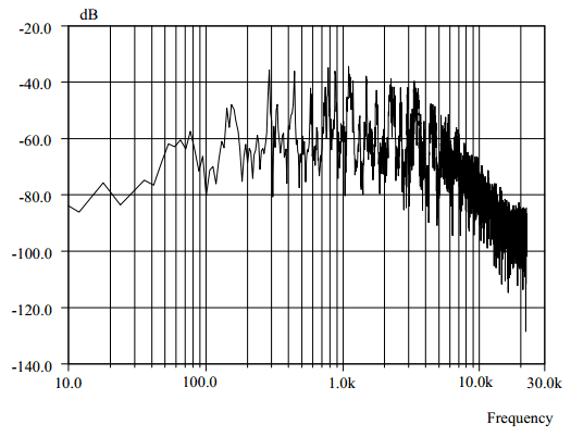
On the same audio fragments, a Fast Fourier Transform (FFT) was performed over the full length. A normal log-log bode plot of the frequency content (Picture 4) does not provide very useful information.


Picture 4: Traditional graph of a Fourier transform of a music fragment (Vertical scale dB’s are relative to full scale for measurement bandwidth 2/Tfragment)


Firstly, there is no need for a high accuracy, so it seems more logical to choose the vertical scale of the plot linear instead of logarithmic. Secondly, efficiency is a matter of power. When an amplifier has a better efficiency for certain frequencies, it is important to know how much power is present in those frequencies, not how much amplitude. So it’s more useful to square the amplitudes. Finally, the squared FFT gives the power of the frequencies in the signal. The frequencies are linearly spaced. With a logarithmic frequency axis, a temptation exists to overemphasise the lower frequencies because they are relatively enlarged. A linear frequency axis might seem a logical choice, but since pitch perception is logarithmic in nature (every octave higher equals a factor two), it is preferable to use a logarithmic axis, and plot the sum of the squared Fourier coefficients. An extra advantage is that the summation smoothens the curve.
Presented in this way, the frequency distribution is a line that starts at (almost) power = 0 at 20 Hz, climbing to power = 1 at 20 kHz. The frequency distributions of all fragments are shown on Picture 5. The average fragment is S-shaped, with a mid-frequency part corresponding to a straight line between (50 Hz, 0) and (3 kHz, 1). This does not come as a surprise when we realise that the notes in a musical scale are fixed factors in frequency apart, in which case a linear frequency distribution requires all notes to be equally loud. In Picture 5, the fragments with much power in the lower frequencies have a house beat or a contrabass. The fragments with much power in the higher frequencies mostly have electric guitars or synthesisers. One fragment in particular stands out because it contains much more high frequencies than the others. It is the intro of Melissa Etheridge’s "Like the way I do", containing a guitar and a tambourine.


Picture 5: Frequency distribution (of all audio fragments)