The switching electronic assemblies contains elements that are working in switching mode and they can be of non-regenerative or regenerative type. At the non-regenerative assemblies the state of the output is a function of the input signal only, while at the regenerative assemblies the state of the output doesn't depend only on the input signal, but also it depends on the previous state of the assembly. The regenerative assemblies are mostly implemented as two-step amplifiers with strong positive feedback, which allows fast changing of the states of the active amplifiers between the mode of conduction into the mode of stopping or saturation.
Depending on the configuration, the regenerative assemblies can have two stable states, one stable and one quasi-stable (transitional) state or two quasi-stable states.
Bistable multivibrator
Bistable multivibrator (trigger, flip-flop), is a regenerative assembly with two stable states, where the transition from one into another state is performed with step-change under the influence of the trigger (control) signal. The controlling of the trigger can be done with applying short pulses on the transistors bases. If the triggering pulses are generated from one source, then the controlling is called symmetric triggering, and if are used two independent sources, then it's called non-symmetric triggering. In case of non-symmetric triggering, one of the inputs serves as set input for setting the trigger in state Q = 1, and the other input serves as reset input for its deletion, Q = 0.
The trigger circuit shown on Picture 1 is a bistable multivibrator which consists two amplifiers with bipolar transistors (inverters). The two outputs of this circuits are marked as V1 and V2. The output of each inverter serves as a input for the other. In one stable state of the assembly, the transistor Q1 is in saturation, while the transistor Q2 is blocked. For this state, the output V2 is on some positive potential level and the output V1 is near to zero, which is the saturation voltage between the collector and emitter of Q1. In the other stable state Q1 is blocked and Q2 is in saturation, so the output V1 is on some positive level and V2 is near to zero.

Picture 1: Bistable Multivibrator
The speed of the trigger, or the duration of the transition mode which starts with applying of the triggering pulses, in general it depends on the switching parameters of the transistors. So, for the transistors with higher current amplification and lower time constant of its base, which are actually a high-frequency transistors, the speed of the trigger would be higher. The higher speeds of work can also be achieved with lower values of the resistors R1 and R2, but in that case the dissipation of the trigger is increased. However, the regenerative process can be speed up without increasing the dissipation of the trigger, and that's done in our circuit with the capacitors C1 and C2. Adding the capacitors, shunts the resistors R2 and R5 in the transitional mode, so the step changes in the collector are reflected in the base of the other transistor which provides faster commutation or switching of the trigger.
Time-domain analysis
The values of the resistors R1 and R4 are usually equal, which means the trigger is symmetric, and those values are selected for the wanted collector current of saturation. If the resistor values satisfy R2 = R5 = 10*R1 and R3 = R6 = 3*R2, as it is in the case of the circuit on Picture 1, then the reliable operation of the trigger is provided with current amplification factor of 20, which is common feature of any standard bipolar transistor.
It can be noticed that the functionality of the trigger will not be broken if the resistors R3 and R6 are removed, since it would still be satisfied that Vbe > Vce, but in that case it should be provided deeper permeation of the transistors in their region of saturation. In our circuit we choose the power supply voltages of Vcc = Vbb = 12 V.
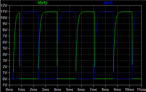
Picture 2: Transient analysis - output voltage V1 and V2 wave forms (time-domain)
The results of the transient analysis for this circuit in time domain is shown on Picture 2. On same picture are plotted both wave forms of the outputs V1 (green line plot) and V2 (blue line plot). The high level of the outputs is about 11 V, while the low level is near to zero or about 17 mV, which is actually the saturation voltage Vce(sat) of the transistors BC547C, the models used in this simulation. The duration of high/low levels is about 1.5 ms, and this value can be altered with different values for the capacitors C1 and C2.
No comments:
Post a Comment